Static logic design for CMOS

a logic and cmos technology, applied in logic circuits, logic circuits characterised by logic functions, pulse techniques, etc., can solve the problems of increasing scaling, low-power, reliable logic circuits, and the optimization of bulk cmos circuits to take full advantage of soi substrate unique properties, and achieve the effect of maximizing the advantages

Active Publication Date: 2005-12-13
TEXAS INSTR INC
View PDF8 Cites 6 Cited by
  • Summary
  • Abstract
  • Description
  • Claims
  • Application Information

AI Technical Summary

Benefits of technology

[0005]The static logic circuit described here maximizes the advantages obtained from using SOI substrates. The instant invention comprises static logic circuits with pull-down networks comprised of PMOS transistors and pull-up networks comprising NMOS transistors. In particular the instant invention is a static logic circuit on a SOI substrate, comprising: a pull-up network comprising a plurality of parallel connected MOS transistors with a first and second common node, wherein at least one of said plurality of parallel connected MOS transistors is a NMOS transistor and at least one of said plurality of parallel connected MOS transistors is a PMOS transistor; a circuit supply voltage which is connected to said first common node of said pull-up network; a pull-down network which is connected to said second common node of said pull-up network; and an output node which is connected to said second common node of said pull-up network. In addition, the pull-down network comprises a plurality of series connected MOS transistors connected to a circuit ground; at least one of said plurality of series connected MOS transistors is a NMOS transistor and at least one of said plurality of series connected MOS transistors is a PMOS transistor; at least one of said MOS transistors in said pull-up network has a gate tied to a floating substrate body and; at least one of said MOS transistors in said pull-down network has a gate tied to a floating substrate body.

Problems solved by technology

Designing small, fast, low-power, and reliable logic circuits is becoming more difficult with scaling.
This circuit layout and design methodology while optimized for bulk CMOS circuits does not take full advantage of the unique properties of SOI substrates.

Method used


Image

  • Static logic design for CMOS
  • Static logic design for CMOS
  • Static logic design for CMOS

Examples


Embodiment Construction

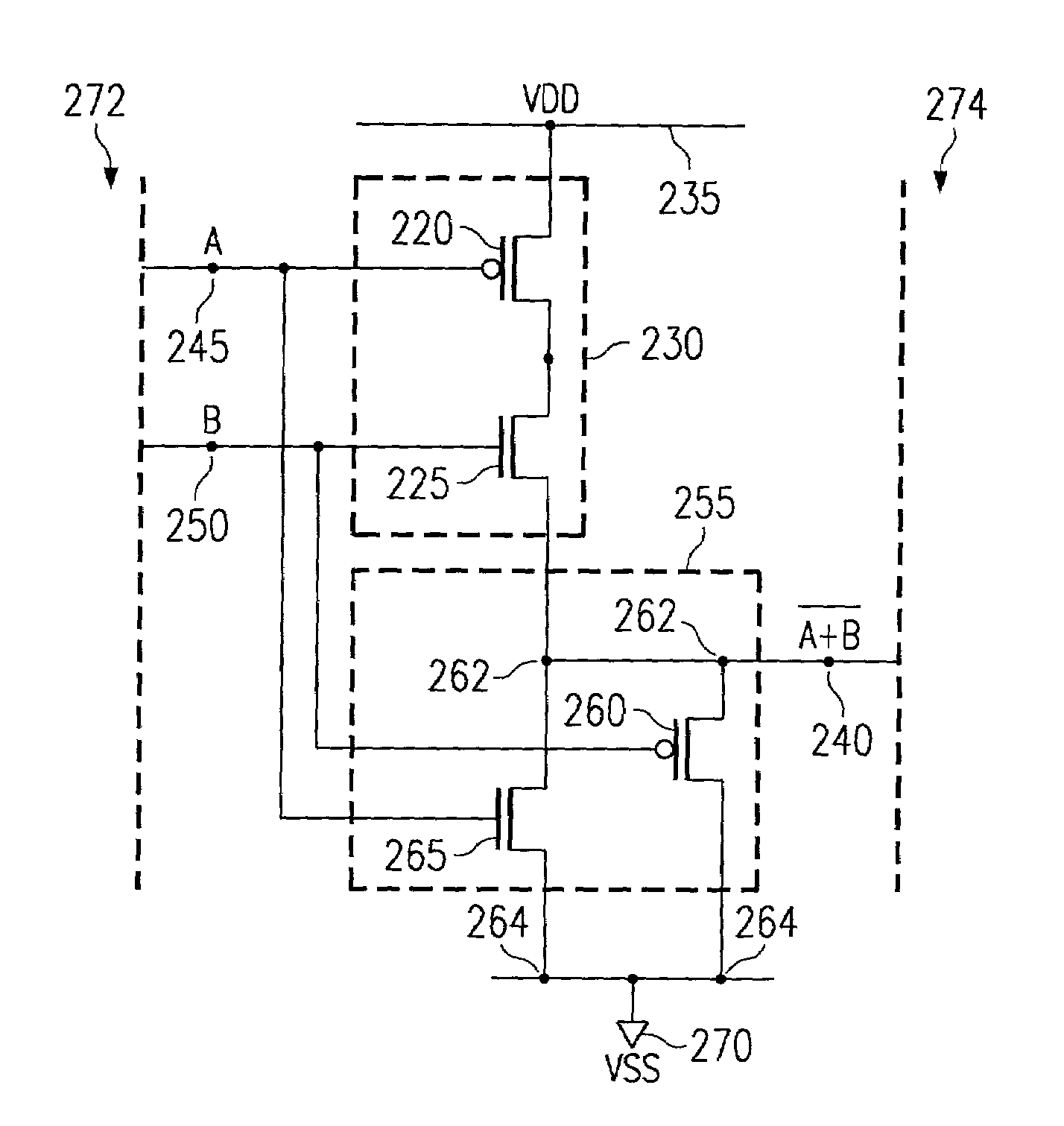
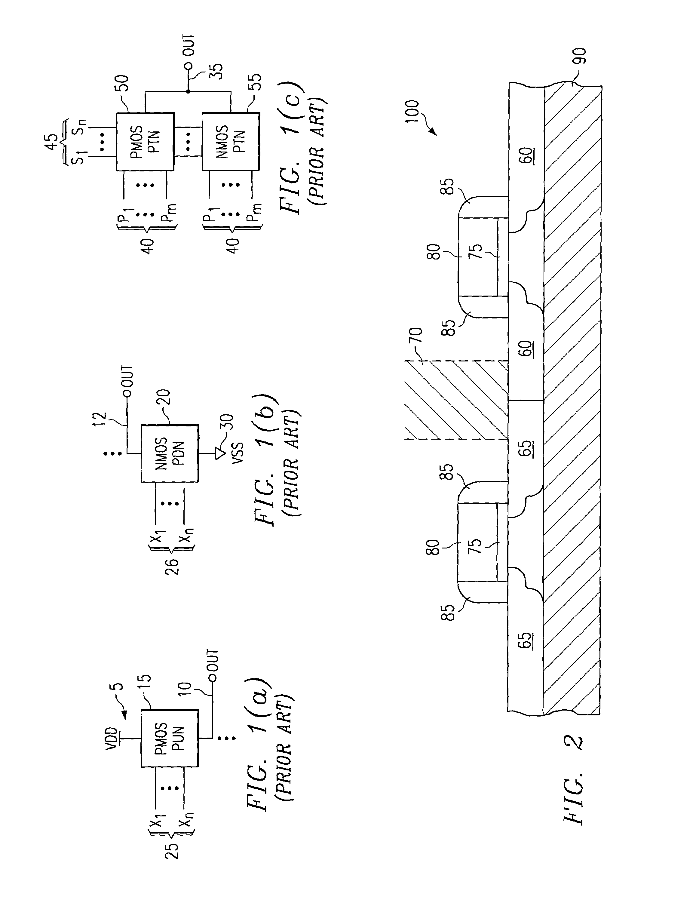
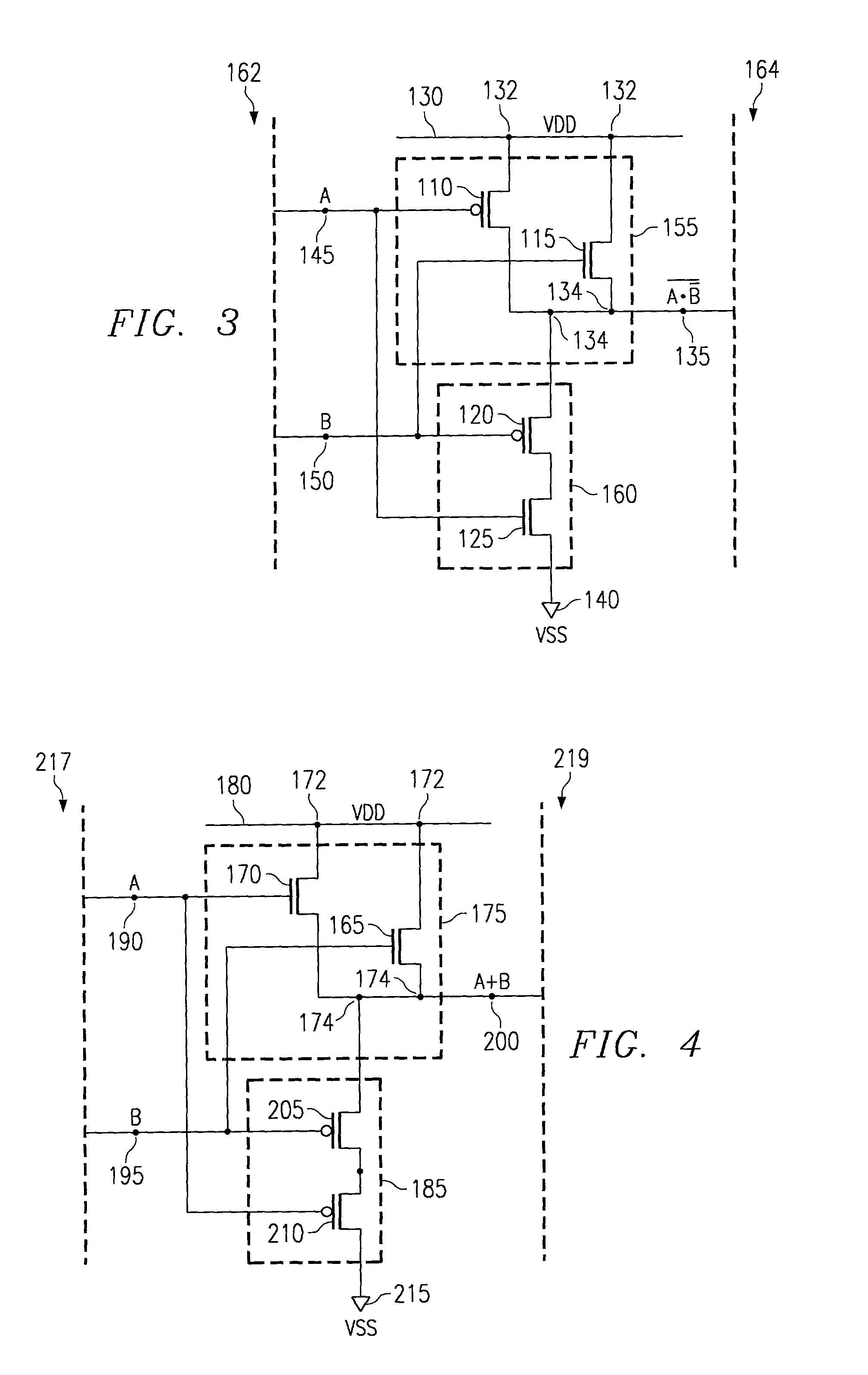
[0014]While the following description of the instant invention revolves around FIGS. 1–6, the instant invention can be utilized in any semiconductor device structure. The methodology of the instant invention provides a design methodology for logic circuits.

[0015]As shown in FIG. 2, the source / drain p-region 60 of a PMOS transistor can abut a source / drain n-region 65 of a NMOS transistor. In this scheme, the contact or silicide 70 that connects the p-region 60 and the n-region 65 can be optional in the “logic” sense if the p-n junction between the p-region 60 and the n-region 65 is never reversed biased. Unlike bulk CMOS technology, therefore, in SOI technology the physical connection of a PMOS transistor and an NMOS transistor along their source / drain regions consumes a silicon area that is compatible to the connection of two NMOS transistors or two PMOS transistors along their source / drain diffusions. Based on this unique property of SOI technology, a new logic for SOI termed here ...


PUM


Abstract

A static logic circuit with a pull-up network (155) and a pull-down network (160). The network is fabricated on SOI substrates and the pull-up network comprises at least one NMOS transistor (115) and the pull down network comprises at least one PMOS transistor (120).

Description

[0001]This application claims priority under 35 U.S.C. § 119(e)(1) of provisional application Ser. No. 60 / 226,178, filed Aug. 18, 2000.FIELD OF THE INVENTION[0002]The invention is generally related to the field of logic circuits and more specifically to a novel design methodology for achieving faster circuits with a more compact circuit layout.BACKGROUND OF THE INVENTION[0003]Designing small, fast, low-power, and reliable logic circuits is becoming more difficult with scaling. Integrated logic circuits on silicon on insulator (SOI) substrates are beginning to find increasing usage in an effort to achieve these goals. SOI refers to a silicon substrate where the top layer (in which the devices are fabricated) is separated from the “bulk” portion of the substrate by a insulator layer. This can be contrasted with bulk silicon substrates which have no buried insulator layer. In bulk CMOS circuits, NMOS transistors are fabricated in p-type wells and PMOS devices are formed in n-type wells...

Claims


Application Information

Patent Timeline
Patent Type & Authority Patents(United States)
IPC IPC(8): H03K19/017H03K19/0948
CPCH03K19/01707H03K19/0948H01L2924/0002H01L2924/00
Inventor DENG, XIAOWEI
Owner TEXAS INSTR INC
Why Eureka
Try Eureka