Component built-in module and method for producing the same

a technology of built-in modules and components, which is applied in the direction of printed circuit non-printed electric components association, sustainable manufacturing/processing, and final product manufacturing, etc., can solve the problems of high reliability but is not suitable for high-density mounting, components such as semiconductors cannot be inspected in a mounted state, and achieves high degree of productivity, enhance strength, and improve yield

Inactive Publication Date: 2005-12-13
TESSERA ADVANCED TECH
View PDF36 Cites 109 Cited by
  • Summary
  • Abstract
  • Description
  • Claims
  • Application Information

AI Technical Summary

Benefits of technology

[0007]Therefore, with the foregoing in mind, it is an object of the present invention to provide a component built-in module that allows a component such as a semiconductor to be inspected as to the mounted state or their properties before embedding, which leads to the improvement of the yields, and moreover can enhance the strength and realize a high degree of productivity and high-density mounting.

Problems solved by technology

However, a conventional glass-epoxy resin impregnation board employs a through-hole structure formed with a drill to form a multilayered circuit, which has a high reliability but is not suitable for high-density mounting.
However, in order to form the passive components inside of a board, there are many problems concerning development of materials, the accuracy of formation, spending on new plant and equipment, and the like, and therefore the speed of the development would be delayed.
Therefore, this method has a problem in that components such as semiconductors cannot be inspected in a mounted state (hereinafter called “mounting inspection”) and cannot be inspected as to their properties (hereinafter called “property inspection”) before embedding.

Method used


Image

  • Component built-in module and method for producing the same
  • Component built-in module and method for producing the same
  • Component built-in module and method for producing the same

Examples


embodiment 1

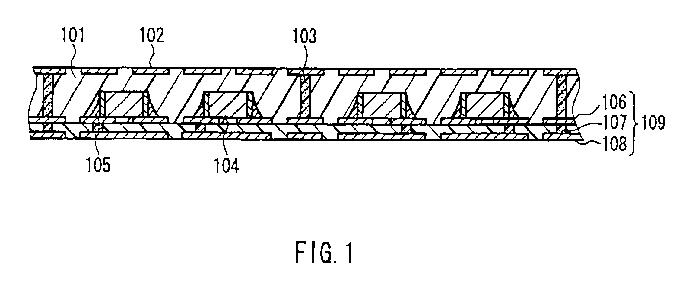
[0041]The following describes embodiments of the present invention, with reference to the drawings. FIG. 1 is a cross-sectional view showing a component built-in module according to Embodiment 1. In FIG. 1, the component built-in module includes an insulating layer 101, a wiring pattern 102, a via 103, a component 104 and a solder 105, and the component built-in module further includes a double-sided board 109 provided with wiring patterns 106 and 108 and an inner via 107.

[0042]As the insulating layer 101, an insulating resin, a mixture of a filler and an insulating resin and the like can be used, for example. It is preferable that the insulating layer contains a resin and a filler, where the percentage of filler content ranges from 50 weight % to 95 weight %, inclusive. The insulating layer also may contain a reinforcing material such as glass cloth. As the insulating resin, a thermosetting resin, a thermoplastic resin, a photo-curing resin and the like can be used. A heat-resistin...

embodiment 2

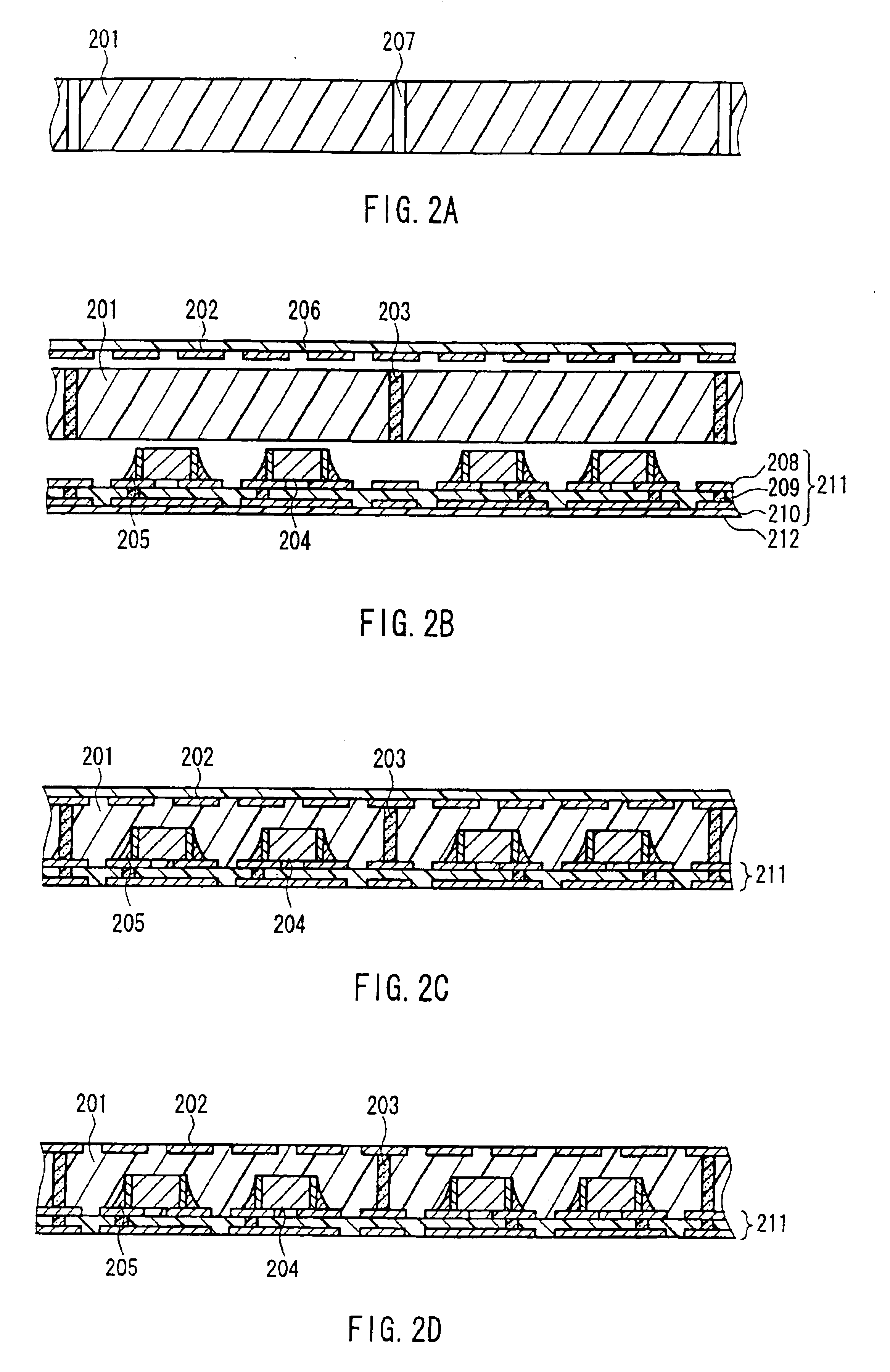
[0049]Embodiment 2 describes one embodiment of a method of producing the component built-in module illustrated in FIG. 1. Materials used in Embodiment 2 are those described in Embodiment 1. FIGS. 2A to 2D are cross-sectional views showing one embodiment of a manufacturing process of the component built-in module. As shown in FIG. 2A, a through hole 207 is formed in an uncured insulating layer 201. As the insulating layer 201, an insulating resin, a mixture of a filler and an insulating resin and the like can be used. First of all, the filler and the insulating resin are mixed and stirred so as to produce an insulating resin mixture in paste form. A solvent may be added to the insulating resin mixture for the purpose of adjusting the viscosity. This insulating resin mixture is shaped into sheet form, whereby the insulating layer 201 can be formed. As a method for shaping the mixture into sheet form, the mixture may be applied to a film using a doctor blade method and the like. The ad...

embodiment 3

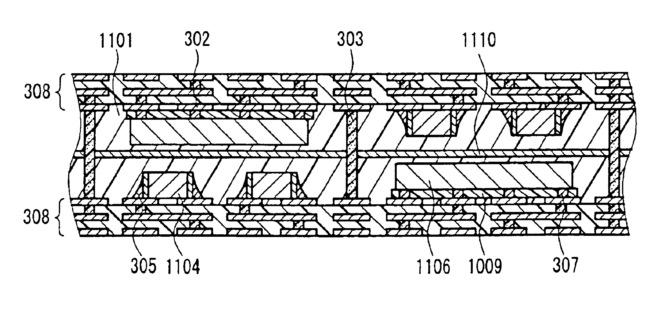
[0057]Embodiment 3 describes one embodiment of a component built-in module. The following describes this embodiment, with reference to FIG. 3. The component built-in module according to this embodiment is the same in the above-stated Embodiment 1 except for a semiconductor 306, a bump 307 and a three-layered wiring board 308. Therefore, materials used in Embodiment 3 are the same as in Embodiments 1 and 2, unless otherwise described. In FIG. 3, the component built-in module includes an insulating layer 301, a wiring pattern 302, a via 303, an electronic component 304, a conductive adhesive 305, the semiconductor 306, the bump 307 and the wiring board 308.

[0058]The semiconductor 306 may be mounted on the wiring board 308 in the same manner as the electronic component 304. By embedding the semiconductor 306 in the insulating layer 301, a high-performance module can be realized. As the semiconductor 306, a semiconductor device such as a transistor, an IC and an LSI can be used. The sem...


PUM


Abstract

A component built-in module includes an insulating layer, wirings integrated with both surfaces of the insulating layer, a via connecting the wirings, and one or more components selected from an electronic component and a semiconductor, which is embedded inside of the insulating layer. In this module, at least one of the wirings is formed on a surface of a wiring board, and the components embedded inside of the insulating layer are mounted on and integrated with the wiring board before embedding. This configuration allows the components such as a semiconductor to undergo a mounting inspection and a property inspection before embedding. As a result, the yields of the module can be improved. In addition, since the components are integrated with the wiring board and embedded, the strength thereof can be enhanced.

Description

BACKGROUND OF THE INVENTION[0001]1. Field of the Invention[0002]The present invention relates to a circuit component built-in module in which a circuit component is arranged in an internal portion of an insulating layer and a method for producing the same.[0003]2. Related Background Art[0004]Recently, with a trend toward high performance and miniaturization of electronic equipment, high-density and high-performance circuit components increasingly have been desired. This leads to a demand for a module with circuit components mounted thereon commensurate with high-performance and high-density. In order to achieve high-density mounting of circuit components, circuit boards currently tend to be multilayered. However, a conventional glass-epoxy resin impregnation board employs a through-hole structure formed with a drill to form a multilayered circuit, which has a high reliability but is not suitable for high-density mounting. Therefore, a multilayered circuit board employing a connectio...

Claims


Application Information

Patent Timeline
Patent Type & Authority Patents(United States)
IPC IPC(8): H01L21/98H01L23/538H01L25/065H01L25/16H05K1/18
CPCH01L21/6835H01L23/5389H01L23/552H01L24/24H01L24/82H01L25/0652H01L25/16H01L25/50H05K1/186H01L24/81H01L24/83H01L2221/68345H01L2224/2402H01L2224/24226H01L2224/8121H01L2224/81815H01L2224/82047H01L2224/83801H01L2224/83851H01L2924/01004H01L2924/01005H01L2924/01009H01L2924/01012H01L2924/01013H01L2924/01029H01L2924/01033H01L2924/01039H01L2924/01046H01L2924/01075H01L2924/01078H01L2924/01079H01L2924/01082H01L2924/09701H01L2924/19041H01L2924/19042H01L2924/19043H01L2924/19105H01L2924/30105H01L2924/30107H01L2924/3025H05K3/20H05K3/4069H05K3/4602H05K3/4652H05K2201/10378H05K2201/10636H05K2203/061H01L2224/16225H01L2224/32225H01L2224/73204H01L2924/01006H01L2924/01047H01L2924/014H01L2924/00H01L2224/2929H01L2224/293H01L2924/00011H01L2224/29075H01L2924/15787H01L2924/12042Y02P70/50H05K1/18
Inventor ASAHI, TOSHIYUKISUGAYA, YASUHIROKOMATSU, SHINGOYAMAMOTO, YOSHIYUKINAKATANI, SEIICHI
Owner TESSERA ADVANCED TECH
Why Eureka
Try Eureka