
Self-repairing integrated circuit and method of operating the same

Active Publication Date: 2005-12-13
AVAGO TECH INT SALES PTE LTD
View PDF4 Cites 9 Cited by
  • Summary
  • Abstract
  • Description
  • Claims
  • Application Information

AI Technical Summary

Benefits of technology

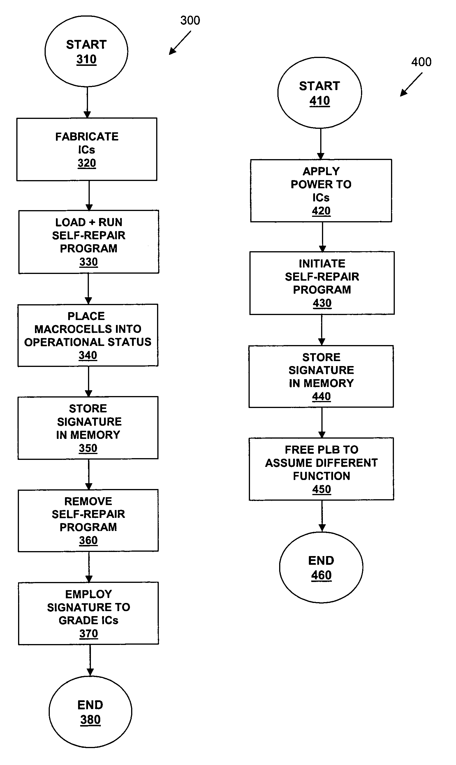
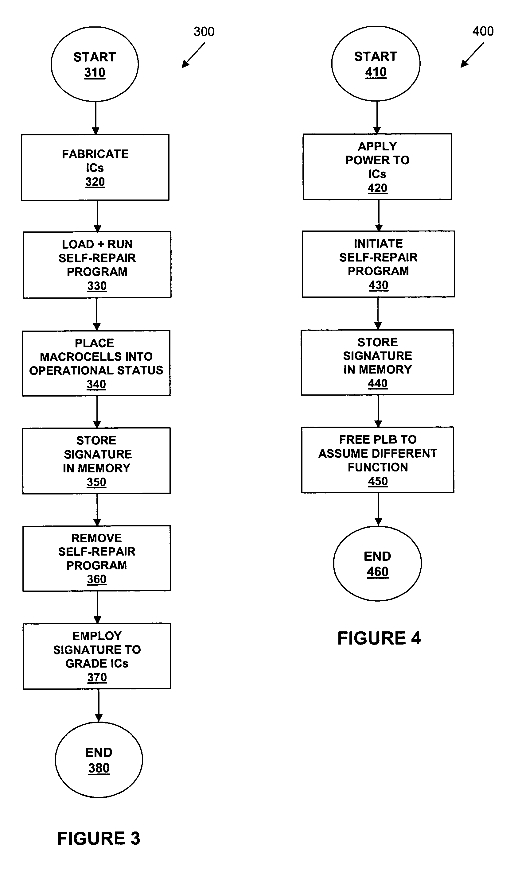
[0017]PLBs are also more flexible than hard-coded logic, allowing them to be potentially reused in another capacity when testing is complete. Thus, in one embodiment of the present invention, the self-repair program is capable of being dissociated from the PLB to allow the PLB to assume a different function in the IC.
[0019]In one embodiment of the present invention, the self-repair program causes the PLB to test all of the plurality. In an embodiment to be illustrated and described, the IC comprises more than one plurality of interchangeable hard macrocells, and the self-repair program causes the PLB to test at least some of each of the more than one plurality. Sufficient numbers of functioning hard macrocells are placed into an operational status such that the IC can operate properly.

Problems solved by technology

Because of the increasing complexity of new designs, test development costs now account for a large percentage of the total ASIC development cost.
This testing is necessary because perfect yields are difficult to achieve.
It is not uncommon for a certain percentage of unpackaged ASICs to contain hard macrocells that fail testing processes, due largely to non-systemic manufacturing defects and degradation faults.
Such manufacturing issues are likely to increase as process geometries continue to shrink and the density of memory cells increases.
While this strategy does not require any chip area other than some simple multiplexing circuitry, it is limited to on-chip memories and other circuitry accessible via I / O pins.
Another drawback of this approach is that ATE capabilities are generally not available to end users once the devices have been shipped, making difficult the task of detecting faults occurring after shipment.
However, such techniques are limited to one-time repair and require significant capital investment.
Further, these techniques may leave ICs useless if the repaired ASICs become defective after shipment from the manufacturing site (perhaps due to electromigration or other burn-in related defects)—even where test equipment is available to end users, traditional field repairs have been expensive, time consuming and largely impracticable.
Unfortunately, as stated above, both conventional BIST and BISR circuitry takes the form of hard-wired logic, which invariably occupies chip area that could otherwise be employed by circuitry useful in the normal operation of the ASIC.
Further, if the BIST or BISR circuitry itself is manufactured with a fault, its operation may be significantly altered, potentially compromising or prohibiting any test or repair function it would be tasked with performing.

Method used


Image

  • Self-repairing integrated circuit and method of operating the same
  • Self-repairing integrated circuit and method of operating the same
  • Self-repairing integrated circuit and method of operating the same

Examples


Embodiment Construction

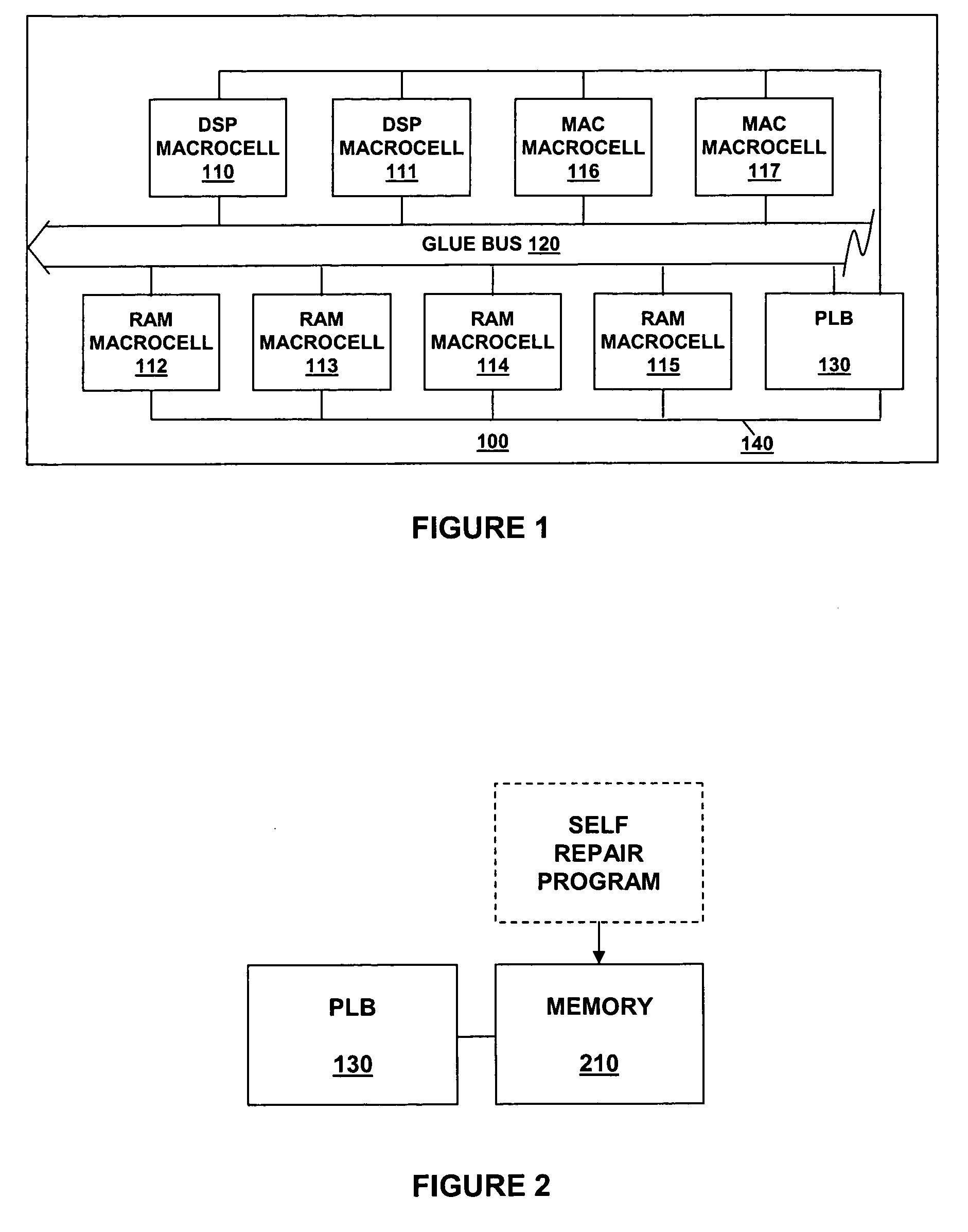
[0028]Referring initially to FIG. 1, illustrated is a block diagram of an ASIC, generally designated 100, incorporating a PLB and self-repair program constructed according to the principles of the present invention. Those skilled in the pertinent art should understand that the ASIC 100 could be a WSI. Those skilled in the pertinent art should also understand that the scope of the present invention encompasses ICs of lesser scales of integration than VLSI.

[0029]The ASIC 100 is illustrated as including a plurality of hard macrocells 110, 111, 112, 113, 114, 115, 116, 117. The hard macrocells 110, 111 are interchangeable DSP hard macrocells. The hard macrocells 112, 113, 114, 115 are interchangeable RAM hard macrocells. The hard macrocells 116, 117 are interchangeable MAC hard macrocells.

[0030]A glue bus 120 interconnects the hard macrocells 110, 111, 112, 113, 114, 115, 116, 117, allowing activated ones of the hard macrocells 110, 111, 112, 113, 114, 115, 116, 117 to communicate with ...


PUM


Abstract

An integrated circuit (IC) and methods of manufacturing and operating ICs. In one embodiment, the IC includes: (1) a plurality of interchangeable hard macrocells, (2) at least one programmable logic block (PLB), (3) a bus intercoupling said plurality and said at least one programmable logic block and (4) a self-repair program, associated with said at least one programmable logic block, that causes said PLB to test at least some of said plurality and place at least a functioning one of said plurality into an operational status.

Description

TECHNICAL FIELD OF THE INVENTION[0001]The present invention is directed, in general, to integrated circuits (ICs) and, more specifically, to a self- repairing very large scale ICs (VLSIs) and wafer-scale ICs (WSIs) and a method of operating such VLSIs or WSIs to achieve self-repair.BACKGROUND OF THE INVENTION[0002]ICs have become key components of many consumer and commercial electronic products, often replacing discrete components and enhancing functionality. The semiconductor processing technologies that produce these ICs have advanced to the point where complete systems, including memories, can be reduced to a single IC or application-specific IC (ASIC). ASICs are usually made up of standard functional units, called “hard marcrocells” or sometimes “IP blocks,” and buses and logic (so-called “glue logic”) that tie the hard-macrocells together. It is a common practice for the manufacturers of such ICs to thoroughly test device functionality at the manufacturing site. Because of the...

Claims


Application Information

Patent Timeline
IPC IPC(8): G01R31/28G06F11/00G11C29/00
CPCG01R31/3187G11C29/4401
Inventor VAIDA, THEODORE F.
Owner AVAGO TECH INT SALES PTE LTD
Learn More