Alternating phase shift mask

a phase shift mask and alternating technology, applied in the field of photolithography technology, can solve the problems of worse critical dimension (cd) control at the edge of the dram array, further reduction in size and density, and difficult realization of further reduction in density, so as to achieve easy arranging and compensate deformation

Inactive Publication Date: 2005-12-20
WINBOND ELECTRONICS CORP
View PDF4 Cites 12 Cited by
  • Summary
  • Abstract
  • Description
  • Claims
  • Application Information

AI Technical Summary

Benefits of technology

[0020]Unlike conventional alternating phase shift mask, phase interference enhancement feature is easily arranged in the alternating phase shift mask. That is to say, it is not necessary to strictly control the phase interference enhancement feature in its shape, dimension, and the position according to the invention. Therefore, the deformation can be compensated without repeated engineering efforts.

Problems solved by technology

As the size of the chips decreases, optical phenomena such as diffraction and interference become increasingly important as they can adversely affect the resolution of the photolithography rendering further reduction in size and increases in density more difficult to realize.
This can result in worse critical dimension (CD) control at the DRAM array edge.

Method used


Image

  • Alternating phase shift mask
  • Alternating phase shift mask
  • Alternating phase shift mask

Examples


Embodiment Construction

[0029]The following description will explain the alternating phase shift mask according to the embodiment of the invention, which proceeds with reference to the accompanying drawings.

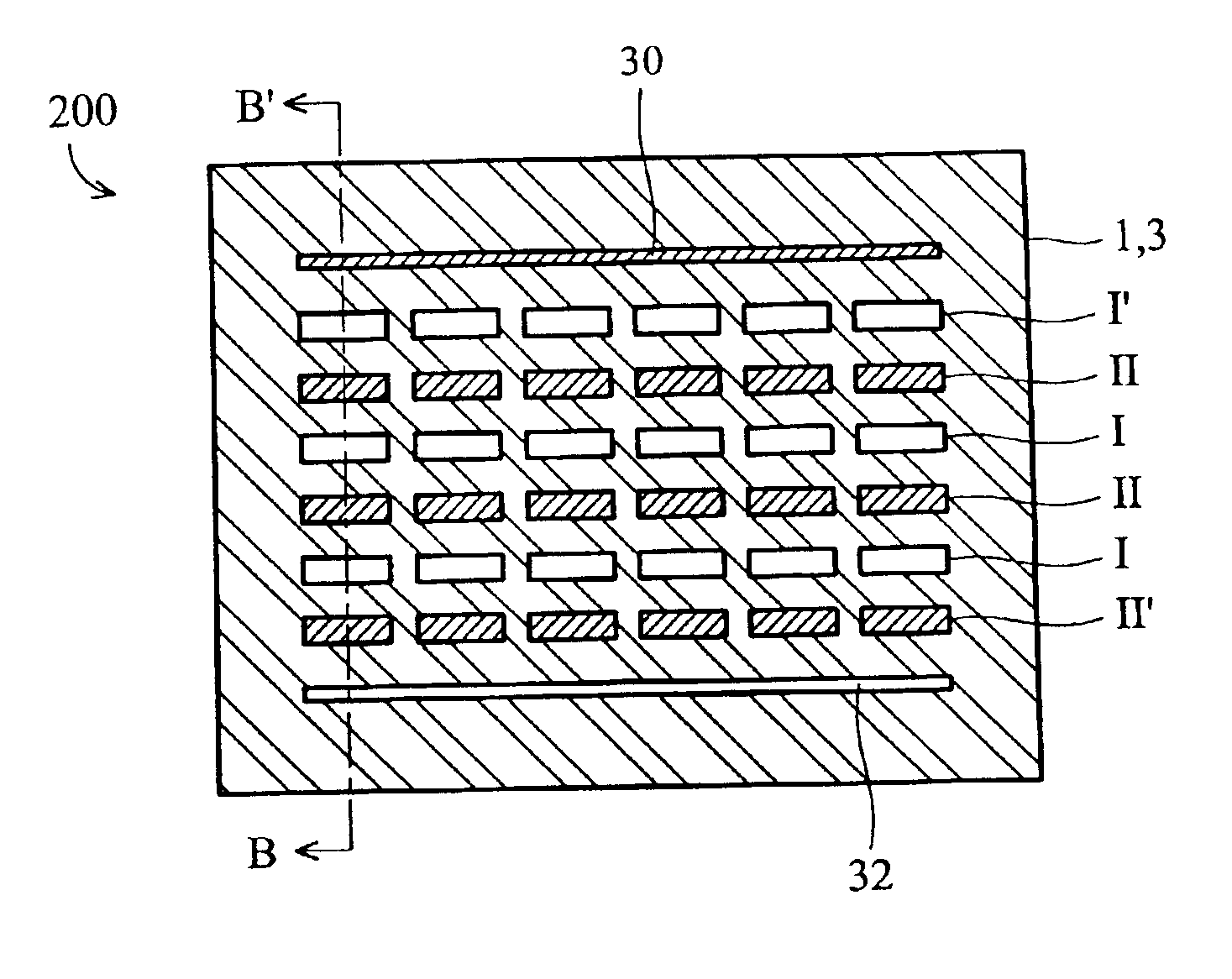
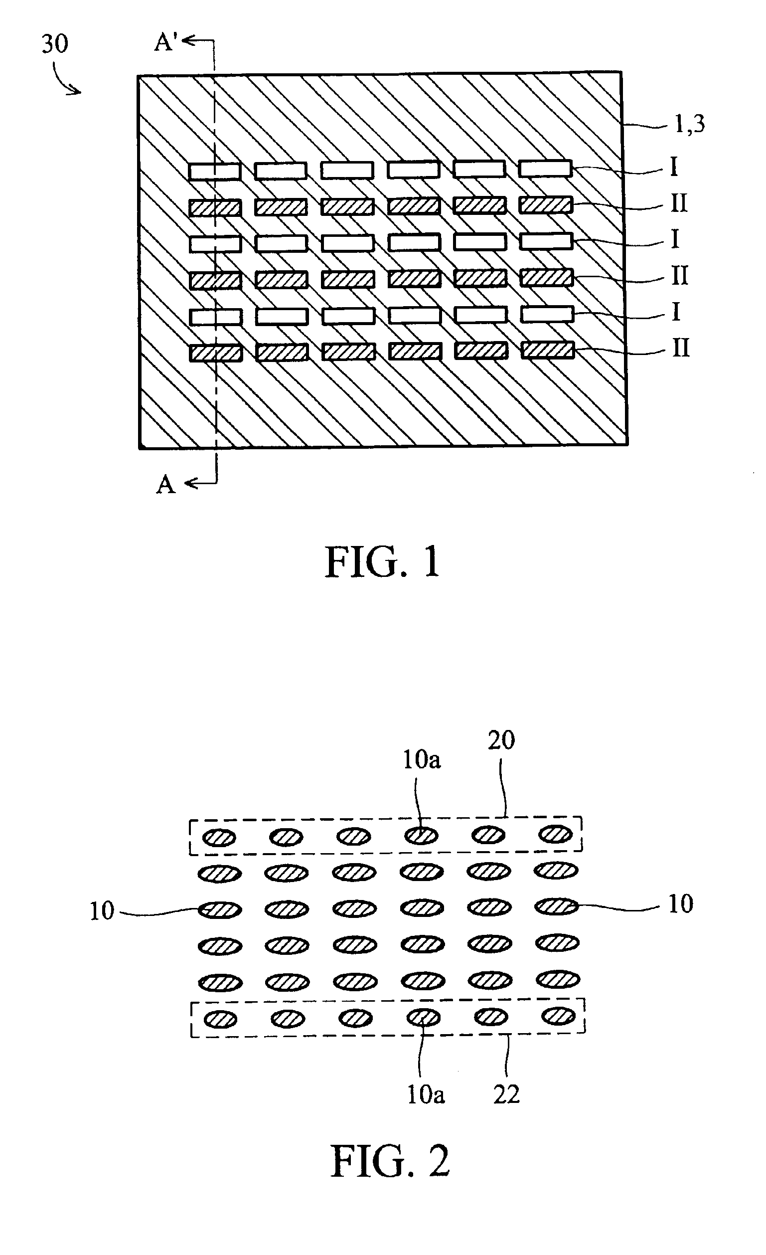
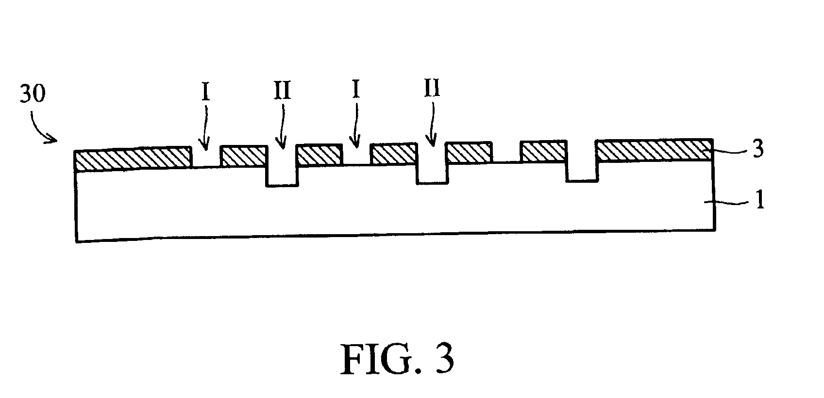
[0030]FIG. 4 and FIG. 6 show an alternating phase shift mask 200 according to the embodiment of the invention. The alternating phase shift mask 200 includes a transparent substrate 1 consisting of quartz materials and a chromium light-shielding layer 3 disposed on the transparent substrate 1. The light-shielding layer 3 has a transparent array consisting of a plurality of first phase (0 degree) rows I and a plurality of second phase (180 degree) rows II alternately interposed between the first phase rows I. The transparent substrate 1 is partially etched to form recesses having a predetermined depth serving as second phase rows as shown in FIG. 6. The transparent array is used to define repeated patterns such as storage nodes of dynamic random access memories (DRAMs) in deep submicron processes, about 0...


PUM

PropertyMeasurementUnit
widthaaaaaaaaaa
widthaaaaaaaaaa
distanceaaaaaaaaaa

Abstract

An alternating phase shift mask. The alternating phase shift mask includes a transparent substrate, a light-shielding layer disposed on the transparent substrate to define a transparent array consisting of a plurality of first phase rows and a plurality of second phase rows alternately interposed between the first phase rows. The alternating phase shift mask further comprises a phase interference enhancement feature disposed a predetermined distance from the outermost row of the transparent array, wherein the phases of the phase interference enhancement feature and the outermost row are reverse.

Description

[0001]Pursuant to 35 U.S.C. § 119(a)-(d), this application claims priority from Taiwanese application no. 091100666, filed on Jan. 17, 2001.BACKGROUND OF THE INVENTION[0002]1. Field of the Invention[0003]The present invention relates to a photolithography technology to fabricate semiconductor devices, more particularly, to an alternating phase shift mask (alt. PSM) capable of reducing or eliminating pattern deformation without repeated engineering efforts.[0004]2. Description of the Related Art[0005]Photolithography is widely used in the semiconductor industry to form a wide range of structures in integrated circuit chips. As the size of the chips decreases, optical phenomena such as diffraction and interference become increasingly important as they can adversely affect the resolution of the photolithography rendering further reduction in size and increases in density more difficult to realize. To minimize such phenomena and extend the range of photolithography, a technique known as...

Claims


Application Information

Patent Timeline
Patent Type & Authority Patents(United States)
IPC IPC(8): G03F1/30G03F1/68H01L21/027
CPCG03F1/30G03F1/144
Inventor SHIAH, CHII-MINGHSU, YI-YUTUNG, YU-CHENGLIAO, HUNG-YUEHTSAI, KAO-TSAIWANG, JONG-BOR
Owner WINBOND ELECTRONICS CORP
Why Eureka
Try Eureka