Modules integrating MEMS devices with pre-processed electronic circuitry, and methods for fabricating such modules

a technology of electronic circuitry and modules, applied in the field of composite structures or modules, can solve the problems of large footprint, inferior performance, and extensive compromises in both circuit and mems device processing

Active Publication Date: 2005-12-27
TELEDYNE SCI & IMAGING
View PDF19 Cites 50 Cited by
  • Summary
  • Abstract
  • Description
  • Claims
  • Application Information

AI Technical Summary

Benefits of technology

[0006]The present invention provides a versatile, compact, low-cost module integrating at least one MEMS device with related electronic circuitry, and a method for making ...

Problems solved by technology

For example, MCM results in large footprints and inferior performance and, although monolithic integration provides re...

Method used


Image

  • Modules integrating MEMS devices with pre-processed electronic circuitry, and methods for fabricating such modules
  • Modules integrating MEMS devices with pre-processed electronic circuitry, and methods for fabricating such modules
  • Modules integrating MEMS devices with pre-processed electronic circuitry, and methods for fabricating such modules

Examples


Embodiment Construction

[0020]The following description presents preferred embodiments of the invention representing the best mode contemplated for practicing the invention. This description is not to be taken in a limiting sense but is made merely for the purpose of describing the general principles of the invention whose scope is defined by the appended claims.

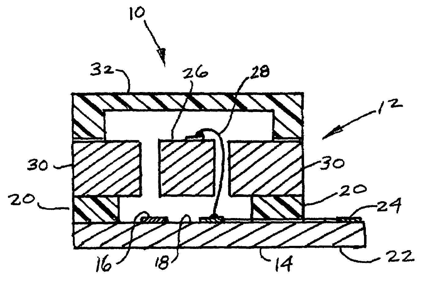
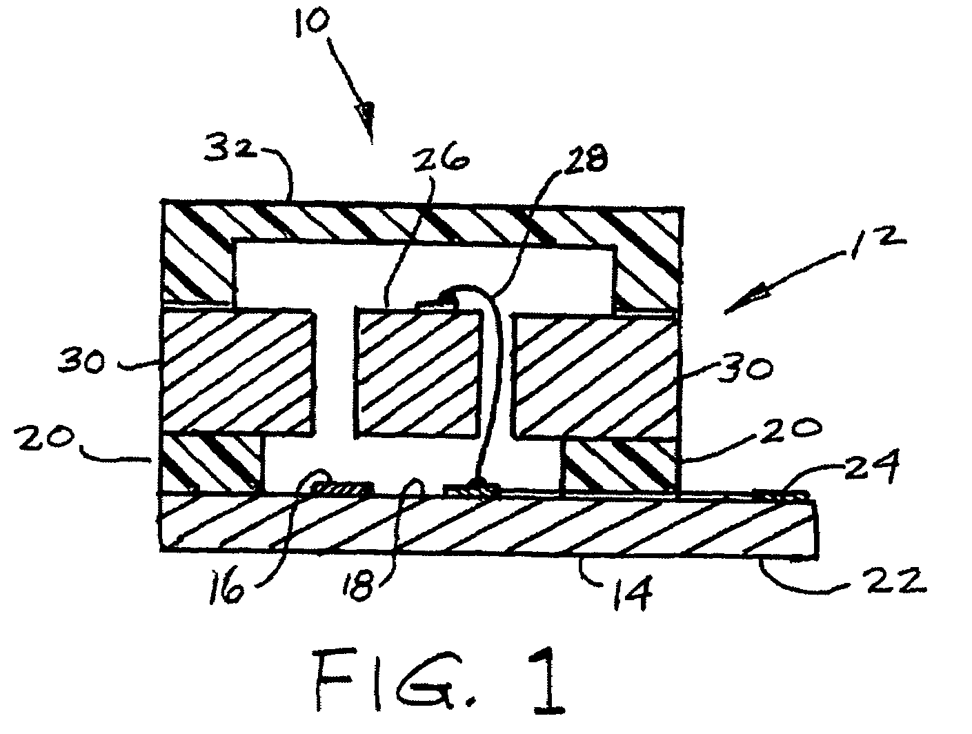
[0021]FIG. 1 illustrates, in schematic form, a module 10 in accordance with one embodiment of the present invention. The module 10 integrates a single MEMS device 12 with a substrate or wafer 14 carrying pre-processed electronic circuitry, shown schematically as a block 16, occupying an area on an upper surface 18 of the wafer 14. The electronics wafer 14 may be in the form of, by way of example, a CMOS die, and the pre-processed circuitry may comprise control, readout / signal conditioning, and / or signal processing circuitry. The MEMS device 12 is attached to the upper surface of the electronics wafer 14 by means of an adhesive bonding agent 20,...


PUM


Abstract

A MEMS module is provided comprising at least one MEMS device adhesively bonded to a substrate or wafer, such as a CMOS die, carrying pre-processed electronic circuitry. The at least one MEMS device, which may comprise a sensor or an actuator, may thus be integrated with related control, readout/signal conditioning, and/or signal processing circuitry.
An example of a method pursuant to the invention comprises the adhesive bonding of a pre-processed electronics substrate or wafer to a layered structure preferably in the form of a silicon-on-insulator (SOI) substrate. The SOI is then bulk micromachined to selectively remove portions thereof to define the MEMS device. Prior to release of the MEMS device, the device and the associated electronic circuitry are electrically interconnected, for example, by wire bonds or metallized vias.

Description

BACKGROUND OF THE INVENTION[0001]1. Field of the Invention[0002]The present invention relates generally to microelectromechanical systems (MEMS) and particularly to composite structures or modules integrating at least one MEMS device with a substrate carrying pre-processed electronic circuitry. The invention further relates to methods for fabricating such modules.[0003]2. Description of the Related Art[0004]MEMS devices comprise a class of very small electromechanical devices that combine many of the most desirable aspects of conventional mechanical and solid-state devices while also providing both low insertion losses and high electrical isolation. Unlike a conventional electromechanical device, a MEMS device can be combined with related electronic circuitry. Presently, this is accomplished either by combining the MEMS device and the circuitry in the form of a multi-chip module (MCM) or by monolithically integrating the two. Both have drawbacks. For example, MCM results in large fo...

Claims


Application Information

Patent Timeline
IPC IPC(8): B81B7/02H01L21/00H01L29/84
CPCB81C1/00238H01G5/38H01G5/40H01L2224/48091H01L2924/00014
Inventor BORWICK, III, ROBERT L.DENATALE, JEFFREY F.ANDERSON, ROBERT J.
Owner TELEDYNE SCI & IMAGING
Why Eureka
Try Eureka