Solid image capturing device, lens unit and image capturing apparatus including an optical mask for storing characteristic data

a technology of image capturing and characteristic data, applied in the direction of printers, instruments, color signal processing circuits, etc., can solve the problems of increasing the number of parts, complicated configuration and size, and being unable to cope with such changes immediately

Active Publication Date: 2005-12-27
CHINON INDUSTRIES +2
View PDF15 Cites 9 Cited by
  • Summary
  • Abstract
  • Description
  • Claims
  • Application Information

AI Technical Summary

Benefits of technology

[0010]In order to solve the above problem, an object of the present invention is to provide a solid image capturing device having a lens unit and an image capturing apparatus. These elements are capable of processing not only image

Problems solved by technology

This results in an increased number of parts, a complicated configuration and an increase in size.
This presents a particularly serious problem when a new generation of solid image capturing devices appears on the market to replace olde

Method used


Image

  • Solid image capturing device, lens unit and image capturing apparatus including an optical mask for storing characteristic data
  • Solid image capturing device, lens unit and image capturing apparatus including an optical mask for storing characteristic data
  • Solid image capturing device, lens unit and image capturing apparatus including an optical mask for storing characteristic data

Examples


Embodiment Construction

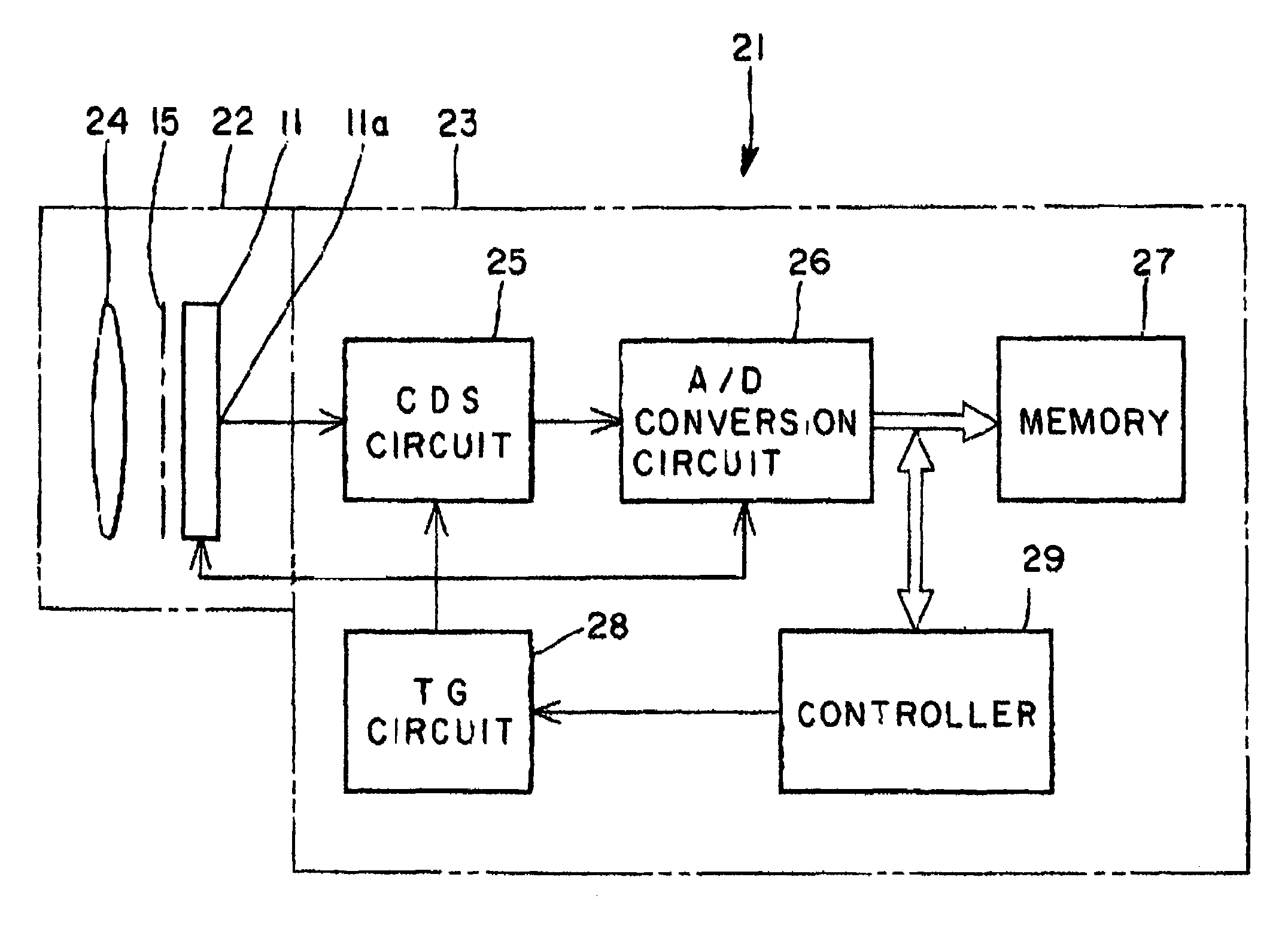
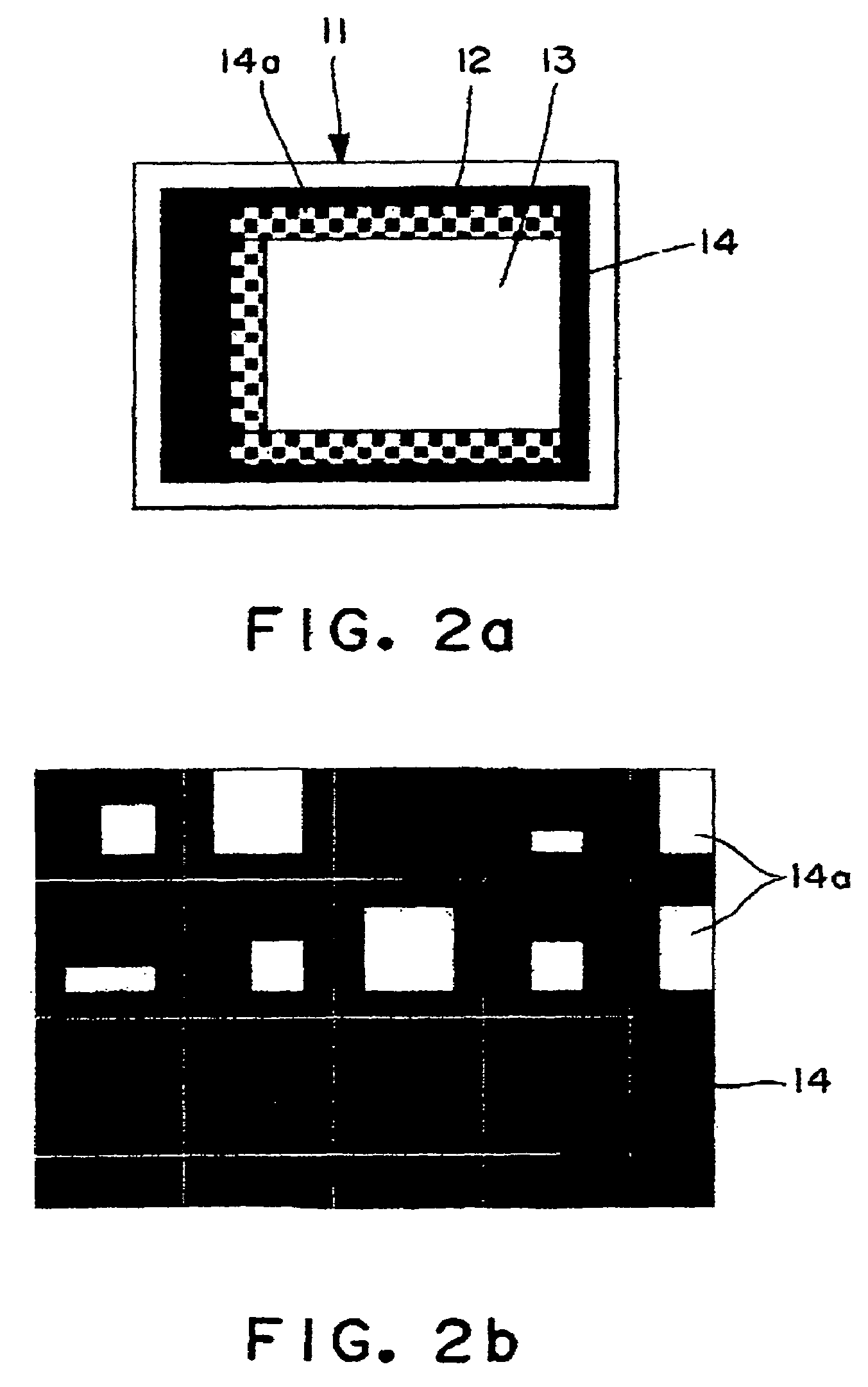
[0041]Referring to FIGS. 1 through 4, a solid image capturing device (image sensor) 11, which may be, for example, a CCD (Charge Coupled Device) or an MOS (Metal Oxide Semiconductor). A square or rectangular image field 12 is formed on the surface of the solid image capturing device 11. A plurality of pixels for conducting photoelectric transfer of light and outputting signals resulting from the transfer are vertically and horizontally arranged in a matrix in the image field 12. The image field 12 has an effective image field 13 used for actually capturing images and an invalid image field 14, which is located outside the effective image field 13 and not actually used for image capture.

[0042]The effective image field 13 and the invalid image field 14 of the image field 12 are defined by an optical mask 15 (see FIG. 1) disposed adjacent to the front face of the solid image capturing device 11. The optical mask 15 has an aperture corresponding to the effective image field 13. A portio...


PUM


Abstract

A solid image capturing device outputs image data and characteristic data of the solid image capturing device on the same output signal line. Both outputs are processed by the same circuit. In one embodiment, the characteristic data is optically stored in the solid image capturing device. In another embodiment, the characteristic data is non-optically stored in the solid image capturing device. The image field of the solid image capturing device includes an invalid image field located outside the effective image field. Signals output from the invalid image field include those concerning the characteristic data of the solid image capturing device.

Description

BACKGROUND OF THE INVENTION[0001]The present invention relates to a solid image capturing device, also called a solid state image capturing device, a lens unit and an image capturing apparatus adapted to be used for image capturing.[0002]Conventionally, a solid image capturing device, e.g. a CCD (Charge Coupled Device) or an MOS (Metal Oxide Semiconductor), is used in an image capturing apparatus, such as a digital camera or a video camera.[0003]Because these solid image capturing devices have their own characteristics, such as defective pixels or the like, it is necessary to correct defects in the pixels or to make other corrections required by the characteristics of each device in order to obtain images of good quality.[0004]For example, Japanese Patent Publication No. 13549 / 1985 discloses an image capturing apparatus which includes a noise eliminating circuit for correcting defective pixels. As shown in FIG. 9, this image capturing apparatus has a CCD 3, which is adapted to condu...

Claims


Application Information

Patent Timeline
IPC IPC(8): G03B17/48H04N5/225H01L27/14H04N5/335H04N5/369H04N5/372
CPCG03B17/48
Inventor ARUGA, URATONAKAMURA, HIDEO
Owner CHINON INDUSTRIES
Why Eureka
Try Eureka