
Optical waveguide device

a waveguide and optical waveguide technology, applied in the field can solve the problems of insufficient inherent performance of each modulator, increased insertion loss, and inability to achieve the design characteristics of optical waveguide devices

Inactive Publication Date: 2005-12-27
SUMITOMO OSAKA CEMENT CO LTD
View PDF19 Cites 0 Cited by
  • Summary
  • Abstract
  • Description
  • Claims
  • Application Information

AI Technical Summary

Benefits of technology

[0009]It is an object of the present invention to improve the performance of an optical waveguide device on which plural elements are monolithically integrated.
[0019]Moreover, it turns out that the buffer layer constituting the optical phase modulator preferably has high density because a DC voltage is not necessary to apply and attenuation of microwave traveling in the electrodes is reduced.
[0021]In the present invention, monolithically integrated optical intensity modulator and the optical phase modulator can exhibit their inherent performances since the buffer layer is composed of a first film and a second film which have preferable physical properties for each modulator, as mentioned in the above example. Therefore, the integrated optical waveguide device can achieve the designed characteristics.
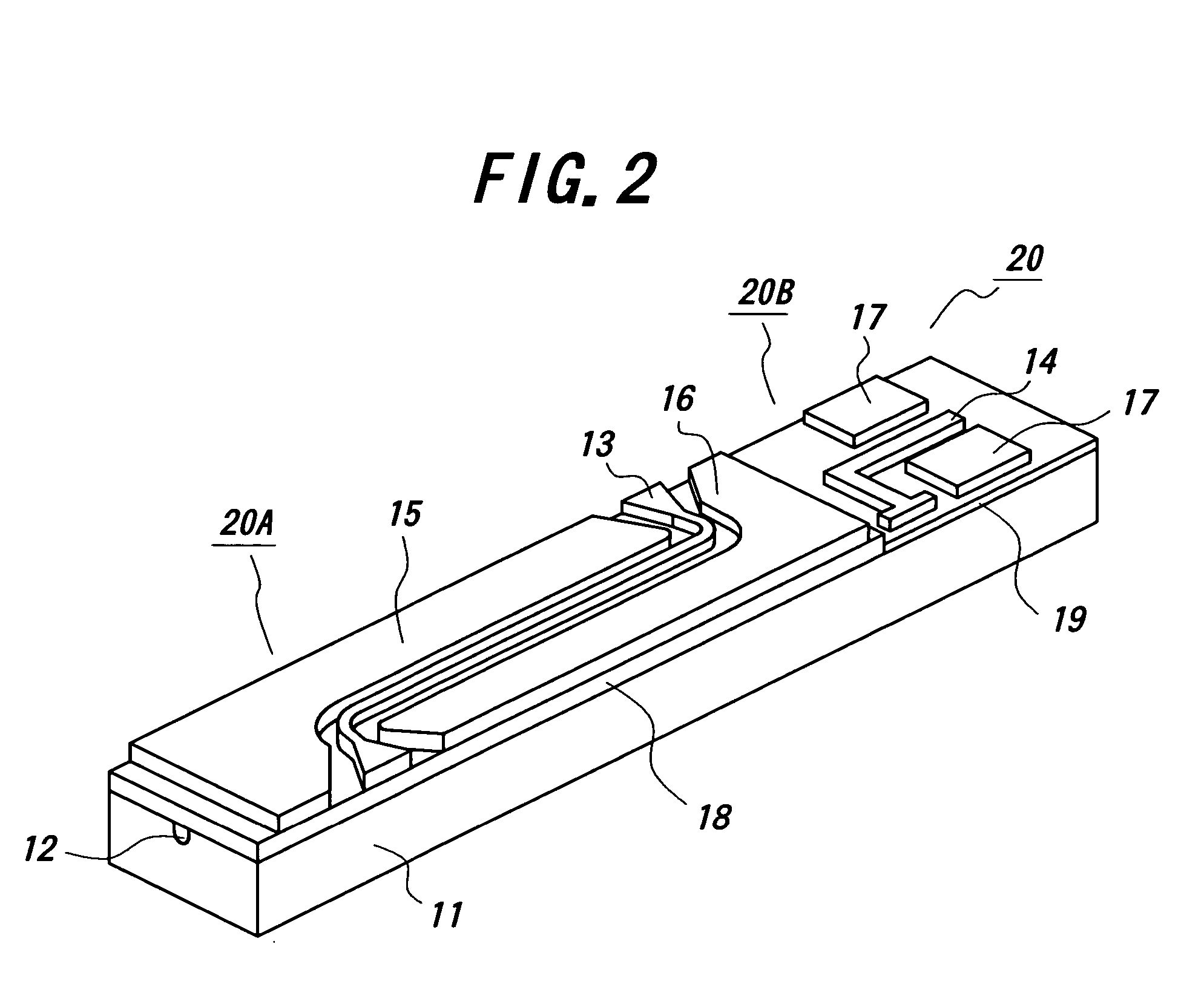
[0023]When the optical phase modulator and the optical intensity modulator are respectively formed on the first film and the second film of the buffer layer, each modulator can exhibit its inherent performance. Therefore, the integrated optical waveguide device can achieve the designed characteristics effectively and efficiently.
[0025]In this case, when the optical phase modulator is formed on the first film and the optical intensity modulator is formed on the second film, each modulator can exhibit its inherent performance sufficiently since the density of the first film can be set much higher than that of the second film, and thus, the optical waveguide device can achieve the designed characteristics more sufficiently.

Problems solved by technology

As mentioned above, there is a trend to install plural optical modulators in the optical fiber communication system, but with the increase of the number of optical modulators, the insertion loss is also increased.
As a result, an optical waveguide device on which an optical intensity modulator and an optical phase modulator are monolithically integrated is completed.
In this case, however, the inherent performance of each modulator can not be often exhibited sufficiently, and therefore, the optical waveguide device can not achieve the designed characteristics.
For example, when a DC voltage is applied to the optical intensity modulator so as to control the operation point, a relatively large DC drift may occur depending on the fabricating condition of the optical intensity modulator, so that the long-term reliability of the optical intensity modulator may be deteriorated.
As a result, when the plural modulators are fabricated on the same substrate to complete an integrated optical waveguide device, as mentioned above, the long-term reliability of the resultant optical waveguide device may be deteriorated.

Method used


Image

  • Optical waveguide device
  • Optical waveguide device
  • Optical waveguide device

Examples


Embodiment Construction

[0009]It is an object of the present invention to improve the performance of an optical waveguide device on which plural elements are monolithically integrated.

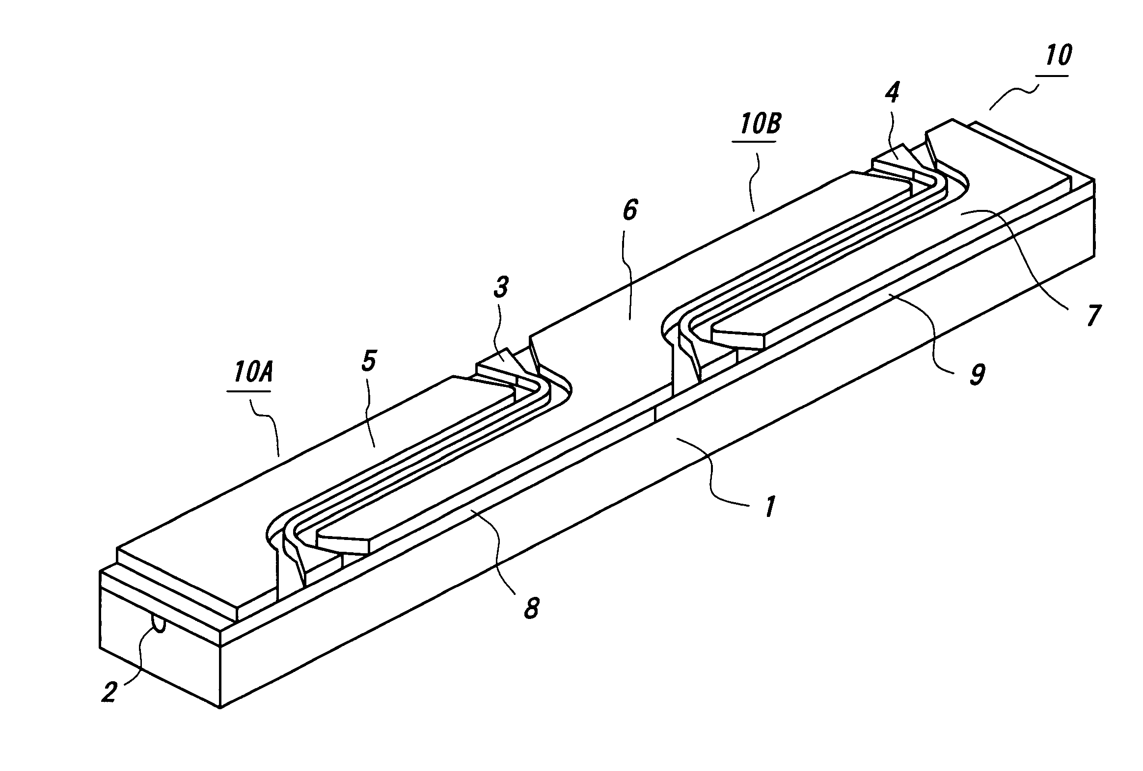
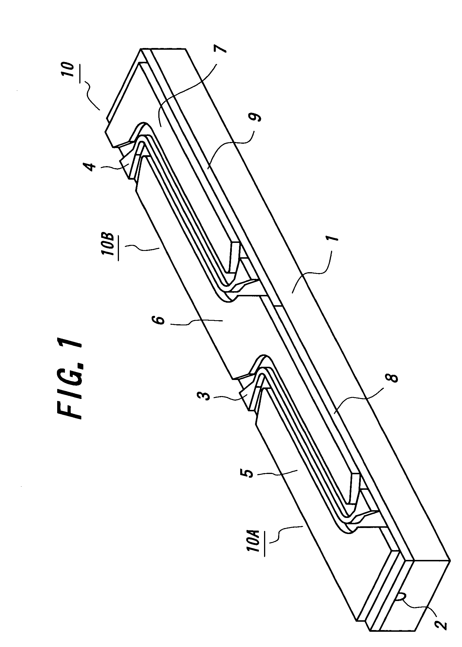
[0010]In order to achieve the above object, this invention relates to an optical waveguide device including:[0011]a substrate having an electro-optic effect,[0012]an optical waveguide formed on the surface of the substrate to guide an optical wave,[0013]a modulation electrode to modulate the optical wave propagating in the optical waveguide, and[0014]a buffer layer which is formed between the substrate and the modulation electrode,[0015]the buffer layer being composed of a first film and a second film in the longitudinal direction of the optical waveguide.

[0016]The inventors had studied intensively to find the cause of the insufficient performance of each modulator in an integrated optical waveguide device on which an optical intensity modulator and an optical phase modulator are monolithically integrated.

[0017]As a result, t...


PUM


Abstract

A first film (8) is formed between a substrate (1) and a signal electrode (3); ground electrodes (5) and (6) which constitute an optical waveguide device (10), and a second film (9) is formed between the substrate (1) and a signal electrode (4); ground electrodes (6) and (7). An optical phase modulator (10A) is composed of the substrate (1), an optical waveguide (2), the signal electrode (3), the ground electrodes (5) and (6), and the first film (8). An optical intensity modulator (10B) is composed of the substrate (1), the optical waveguide (2), the signal electrode (4), the ground electrodes (6) and (7), and the second film (9). The optical waveguide device (10) is composed of the optical phase modulator (10A) and the optical intensity modulator (10B), which are integrated monolithically.

Description

FIELD OF THE INVENTION[0001]This invention relates to an optical waveguide device, on which plural elements with different functions are integrated, and particularly usable for long-haul and high-capacity optical fiber communication systems and optical measuring instruments.BACKGROUND ART[0002]An optical waveguide device comprising of an optical waveguide, a buffer layer and traveling-wave type electrodes which are integrated on a substrate having an electro-optic effect made of lithium niobate (LN) or the like, has been widely employed for long-haul and high-capacity optical fiber communication systems and optical measuring instruments. Particularly, an optical intensity modulator, an optical phase modulator and a polarization scrambler are frequently employed as a key device for optical fiber communication systems.[0003]Recently, with the increase of data traffic due to the rapid advance of the Internet, the optical fiber communication system is required to have faster transmissio...

Claims


Application Information

Patent Timeline
IPC IPC(8): G02F1/03G02F1/035G02B6/12
CPCG02F1/0322G02F1/035G02F1/0356G02F2201/07G02F2201/16G02F2203/21G02F2203/50
Inventor MIYAMA, YASUYUKINAGATA, HIROTOSHISAKAMOTO, TOSHIHIRO
Owner SUMITOMO OSAKA CEMENT CO LTD
Learn More