Imaging device with vertical charge transfer paths having appropriate lengths and/or vent portions

a vertical charge transfer and imaging device technology, applied in the field of solid-state imaging devices and imaging systems, can solve the problems of difficult manufacture of read-out amplifiers with uniform input/output characteristics, troublesome signal processing, and blockage of images, and achieve the effect of easy signal processing

Inactive Publication Date: 2006-01-10
SOVEREIGN PEAK VENTURES LLC
View PDF16 Cites 22 Cited by
  • Summary
  • Abstract
  • Description
  • Claims
  • Application Information

AI Technical Summary

Benefits of technology

[0007]It is therefore an object of the present invention to solve these problems and to provide a structure of a solid-state imaging device that is not so easily influenced by mask misalignments and skewed ion implantation angles during the semiconductor manufacturing process, and in which the signal processing is easy even when signals are read out with a plurality of amplifiers and displayed as one image.

Problems solved by technology

Therefore, misalignments occurring during the masking step in the semiconductor manufacturing process are coupled with the influence of injection angle dependencies during the injection of impurities, and it is difficult to manufacture read-out amplifiers with uniform input / output characteristics.
Differences in the characteristics of the read-out amplifiers lead to the problem that blocks can be observed in the image when replaying the image.
Moreover, when the data that have been read out are combined and displayed as one image, it is necessary to rearrange the image data, which makes the signal processing troublesome.

Method used


Image

  • Imaging device with vertical charge transfer paths having appropriate lengths and/or vent portions
  • Imaging device with vertical charge transfer paths having appropriate lengths and/or vent portions
  • Imaging device with vertical charge transfer paths having appropriate lengths and/or vent portions

Examples


first embodiment

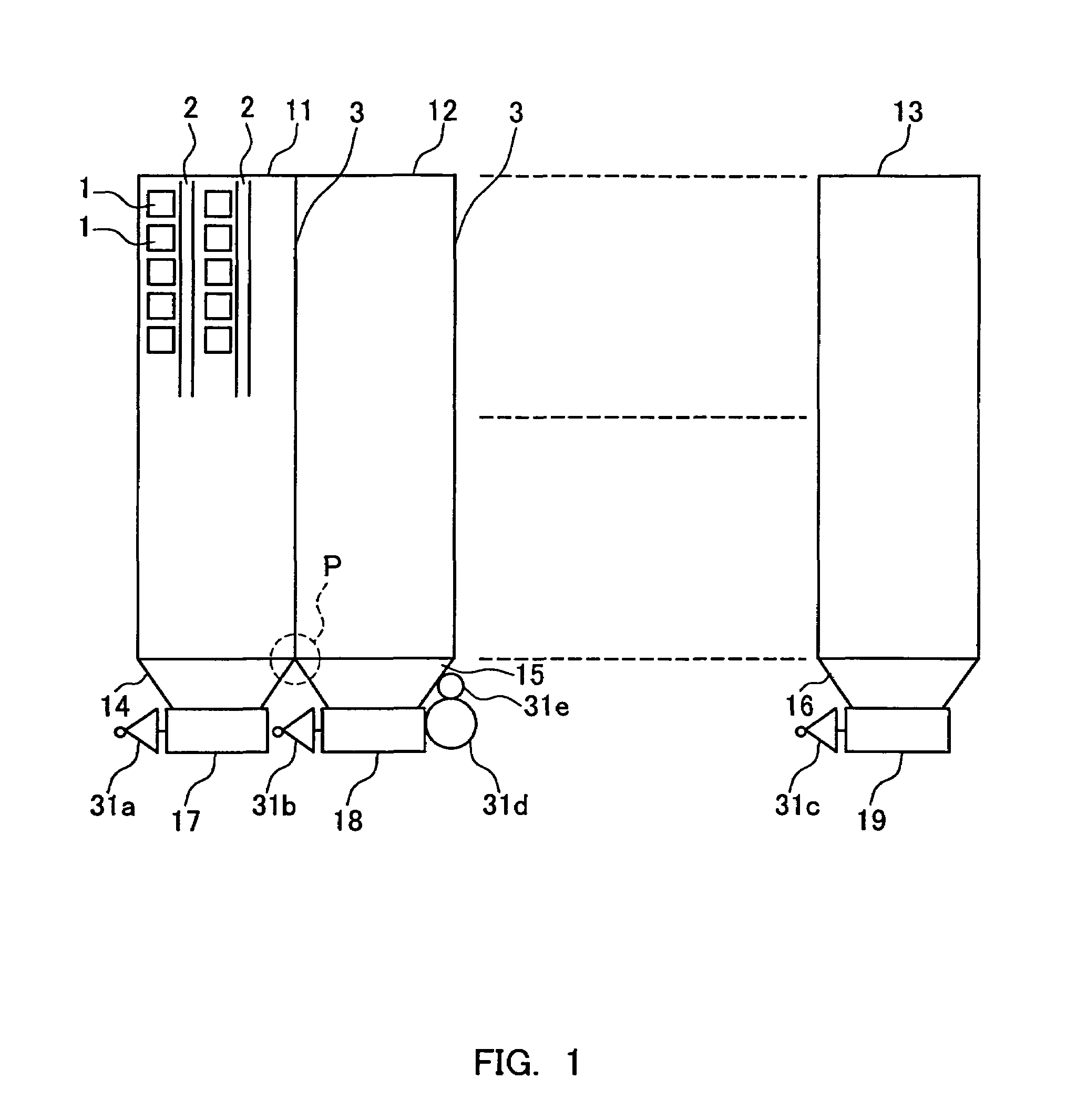
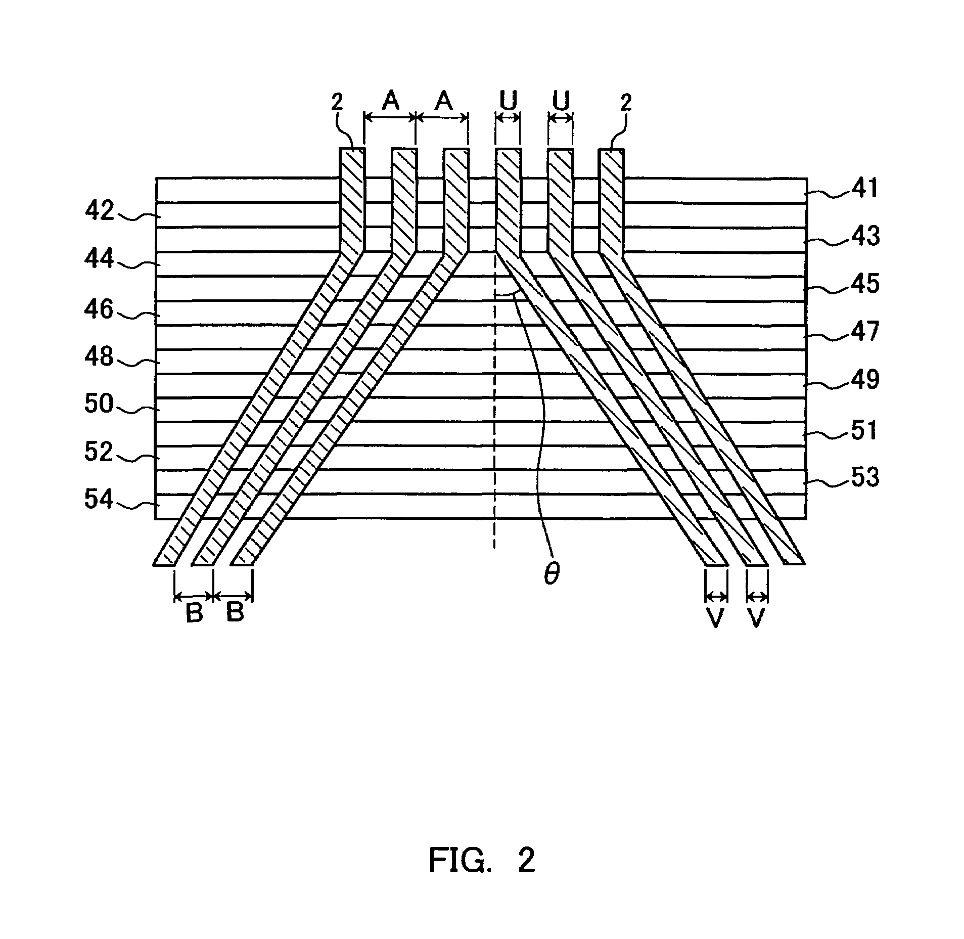
[0030]FIG. 1 shows the configuration of a CCD-type solid-state imaging device in accordance with a first embodiment of the present invention. In this solid-state imaging device, photodiodes (photoelectric conversion portions) 1 are formed in photoelectric conversion blocks 11, 12, . . . , 13, in the form of rows and columns (i.e. a matrix or two-dimensional array). Between the columns of photodiodes, vertical charge transfer paths (VCCD) 2 extend along the columns.

[0031]In this solid-state imaging device, vertical / horizontal conversion portions (V-H conversion portions) 14, 15, . . . , 16 are formed between the photoelectric conversion blocks 11, 12, . . . 13 and the horizontal charge transfer paths (HCCD) 17, 18, . . . , 19. The horizontal charge transfer paths are connected to read-out amplifiers 31a, 31b, . . . , 31c. In this arrangement, the read-out amplifiers are placed in spaces that result from the tapering of the vertical CCDs, so that it is possible to place them directly ...

second embodiment

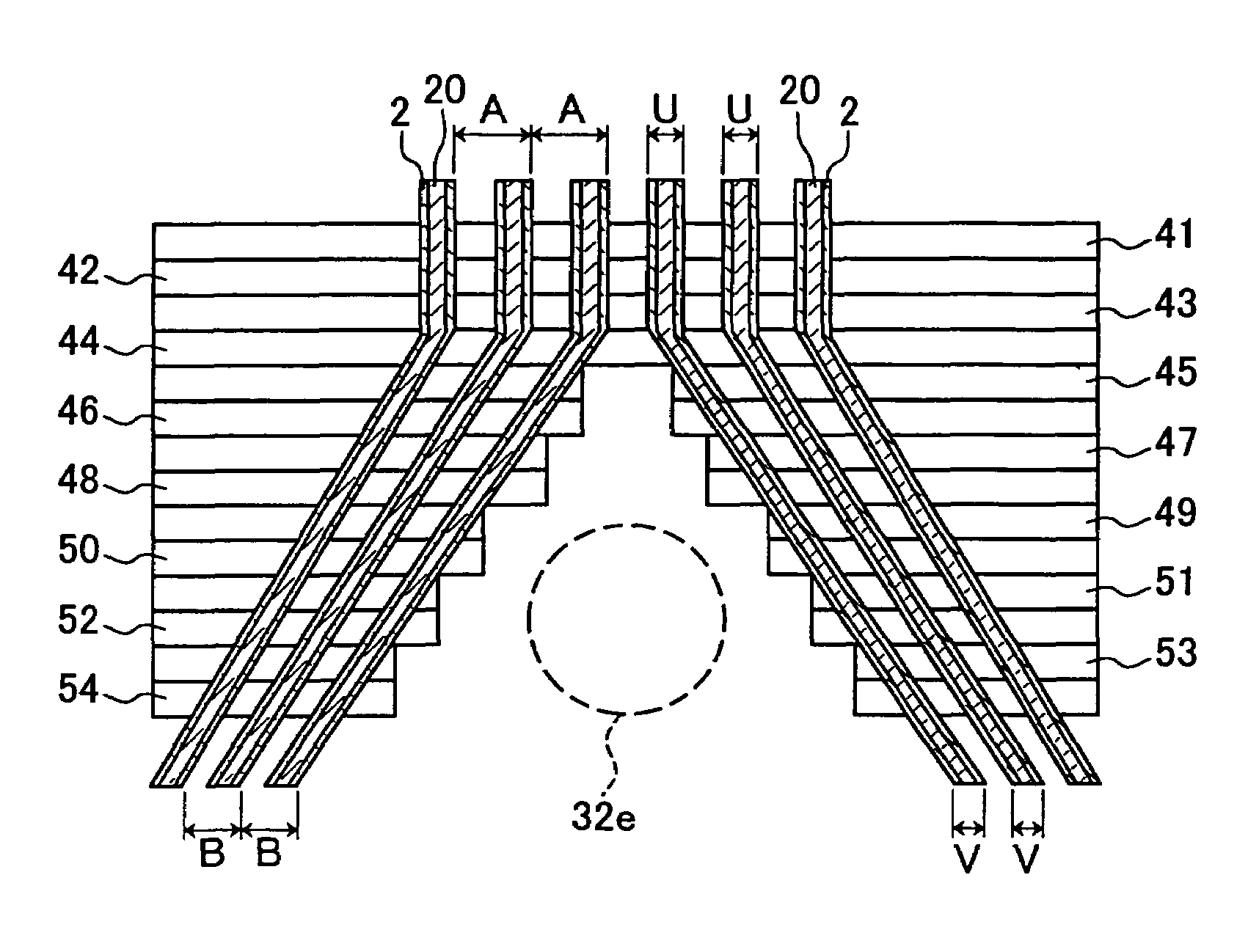
[0039]FIG. 3 shows the configuration of a CCD-type solid-state imaging device in accordance with a second embodiment of the present invention. Also in this solid-state imaging device, as in the first embodiment, the photodiodes 1 and the vertical charge transfer paths 2 are arranged in photoelectric conversion blocks 21, 22, . . . , 23, and horizontal charge transfer paths 27, 28, . . . , 29 and read-out amplifiers 32a, 32b . . . , 32c are provided for each of these photoelectric conversion blocks 21, 22, . . . ,23. V-H conversion portions 24, 25, . . . , 26 are formed between the photoelectric conversion blocks and the horizontal transfer electrodes.

[0040]In this solid-state imaging device, conducting lines 20 are formed along the vertical charge transfer paths 2. These conducting lines 20 feed a driving pulse to the lower transfer electrodes (not shown in the drawing), through contact holes that are formed as appropriate. The contact holes are formed at predetermined spacings corr...


PUM


Abstract

In a solid-state imaging device, a plurality of vertical charge transfer paths is arranged at a horizontal pitch A within a photoelectric conversion region, and at a pitch B that is smaller than the pitch A in a portion where the signals are input into the horizontal charger transfer path. A read-out amplifier and a horizontal charge transfer path for receiving signals from vertical charge transfer paths are provided for each photoelectric conversion block into which the photoelectric conversion region has been partitioned. The read-out amplifiers have the same shape and their positional relation is one of parallel displacement in regions that are obtained by changing the pitch of the vertical charge transfer portions. Thus, a solid-state imaging device is achieved that is not so easily influenced by mask misalignments or skewed ion implantation angles, and in which signal read-out at high speeds is possible.

Description

BACKGROUND OF THE INVENTION[0001]1. Field of the Invention[0002]The present invention relates to solid-state imaging devices and to imaging systems using the same. More particularly, the present invention provides a device structure that is suitable for solid-state imaging devices capable of high-speed read-out.[0003]2. Description of the Related Art[0004]One method of reading out image data at high speeds in an imaging device is to partition the photoelectric conversion region into a plurality of regions, and to read out the charges from these regions in parallel. JP H03-224371A (see FIG. 10), for example, proposes a structure in which the read-out amplifiers are arranged in mirror symmetry (line symmetry). In this solid-state imaging device, signals are output from the pixels arranged in rows and columns in the pixel portions 31 and 32, after having passed through the horizontal charge transfer path 33 and the read-out amplifiers 34 and 35, which are arranged on both ends of the h...

Claims


Application Information

Patent Timeline
Patent Type & Authority Patents(United States)
IPC IPC(8): H04N5/335H01L27/14H01L27/148
CPCH01L27/14806H01L27/14
Inventor MORINAKA, YASUHIROKOMOBUCHI, HIROYOSHIYAMAGUCHI, TAKUMISUZUKI, SEI
Owner SOVEREIGN PEAK VENTURES LLC
Why Eureka
Try Eureka