Scatterometry by phase sensitive reflectometer

a phase sensitive reflectometer and scattering technology, applied in the field of optical devices, can solve the problem of limited measurement resolution of optical imaging systems

Inactive Publication Date: 2006-01-10
TOKYO ELECTRON LTD
View PDF8 Cites 91 Cited by
  • Summary
  • Abstract
  • Description
  • Claims
  • Application Information

AI Technical Summary

Problems solved by technology

The dimensions in the plane of the wafer are obtained from the image; therefore, such measurements are limited by the resolution of the optical imaging system.

Method used


Image

  • Scatterometry by phase sensitive reflectometer
  • Scatterometry by phase sensitive reflectometer
  • Scatterometry by phase sensitive reflectometer

Examples


Embodiment Construction

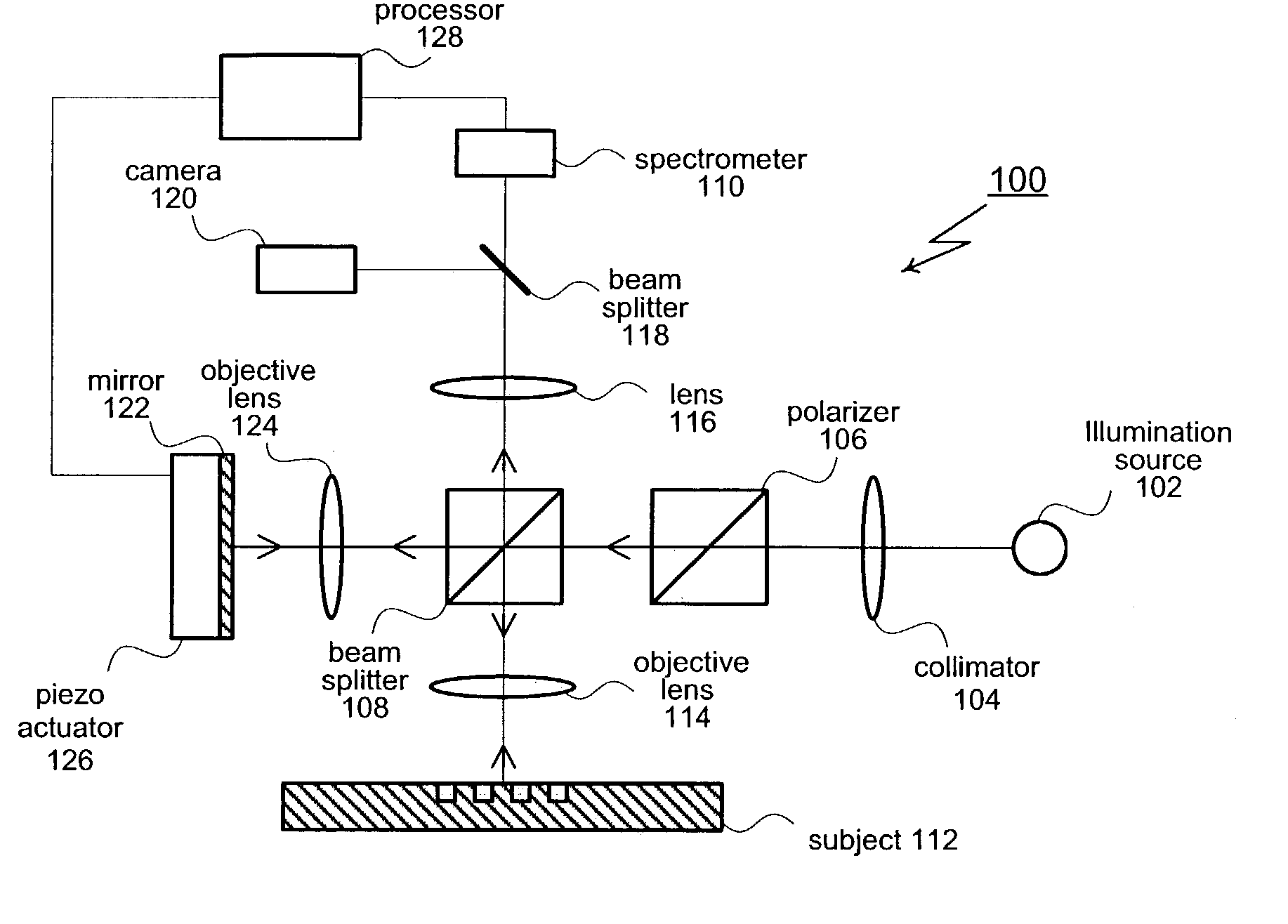
[0019]As shown in FIG. 1, the present invention provides a spectroscopic, phase-sensitive interferometer generally designated 100. Interferometer 100 includes a broadband illumination source 102 that directs a source beam through a collimator 104 and polarizer 106. A beam splitter 108 divides the source beam into separate probe beam and reference beam portions. The probe beam is received by a spectrometer 110 after being reflected by the subject 112 under test (and passing through objectives 114 and 116).

[0020]The probe beam travels along a path that causes it to be reflected by a subject 112 and then received by a spectrometer 110. For this particular implementation, the path traveled by the probe beam includes objective 114, imaging lens 116, and beam splitter 118. Other combinations of optical elements, for example, a reflective objective, are also possible. Typically, the probe beam passes through a system of wavelength dispersive optical elements (not shown) in spectrometer 110...


PUM


Abstract

A phase-sensitive interferometeric broadband reflectometer includes an illumination source for generating an optical beam. A beam splitter or other optical element splits the optical beam into probe beam and reference beam portions. The probe beam is reflected by a subject under test and then rejoined with the reference beam. The combination of the two beams creates an interference pattern that may be modulated by changing the length of the path traveled by the probe or reference beams. The combined beam is received and analyzed by a spectrometer.

Description

TECHNICAL FIELD[0001]The subject invention relates to optical devices used to non-destructively evaluate semiconductor wafers. In particular, the present invention relates to interferometry methods for measuring critical dimensions and film properties.BACKGROUND OF THE INVENTION[0002]As geometries continue to shrink, manufacturers have increasingly turned to optical techniques to perform non-destructive inspection and analysis of semi-conductor wafers. The basis for these techniques is the notion that a subject may be examined by analyzing the reflected energy that results when a probe beam is directed at the subject. Ellipsometry and reflectometry are two examples of commonly used optical techniques. For the specific case of ellipsometry, changes in the polarization state of the probe beam are analyzed. Reflectometry is similar, except that changes in magnitude are analyzed. Scatterometry refers to determining properties of the subject from reflectometry and ellipsometry measuremen...

Claims


Application Information

Patent Timeline
Patent Type & Authority Patents(United States)
IPC IPC(8): G01B9/02G01J3/453
CPCG01J3/453G01B9/0201G01B9/02044G01B9/0209G01B9/02088G01B9/02069G01B11/0675G01B2210/56G01B2290/70
Inventor SEZGINER, ABDURRAHMAN
Owner TOKYO ELECTRON LTD
Why Eureka
Try Eureka