Structure for controlled shock and vibration of electrical interconnects

a technology of electrical interconnections and structures, applied in the direction of electrical apparatus construction details, electrical device connection, printed circuit aspects, etc., can solve the problems of reducing reliability and life expectancy, and affecting the operation of the heat sink. , to achieve the effect of minimizing electrical resistance problems and mechanical failures, preventing or reducing contact motion

Inactive Publication Date: 2006-01-17
IBM CORP
View PDF13 Cites 3 Cited by
  • Summary
  • Abstract
  • Description
  • Claims
  • Application Information

AI Technical Summary

Benefits of technology

[0015]The present invention relates to the prevention or reduction of the contact motion during shock and vibration or other mechanical disturbance of an LGA socket, thereby substantially minimizing electrical resistance problems and mechanical failures between a printed circuit board and a module or other PCB.

Problems solved by technology

Many of the heat sinks have a substantial size and mass relative to the other components.
This size and mass create a moment arm, causing relative movement between the module and the other components when the assembly is subjected to shock or vibration.
In typical LGA applications, shock and vibration can cause a variety of problems which may manifest themselves in decreased reliability and life expectancy, resulting in ongoing maintenance and repair problems.
This increases the friction between the module and the interposer and tends to flatten the two components.
Consequently, it increases stresses within these components, thereby leading to cracks or failures of the module and reduced product life
A flatness of 3 to 6 mils for a ceramic module is common in the industry today, but there is no control over whether the surface is ‘concave’ or ‘convex’.
When this assembly is subject to shock and vibration, the heat sink mass and movement arm tend to ‘rock’ the module in the interposer housing.
This ‘rocking’ creates contact micro-motion, leading to contact wear, and electrical resistance problems.
Contact motion of a small amplitude or micro-motion creates two reliability risks for an electrical contact.
First is the risk of disturbing the contact ‘a’ or asperity spot where electrical contact actually occurs.
Secondly, small amounts of contact motion can wear the plated precious metal layer intended to protect the contact from corrosion.
Another drawback is that there is no protocol for the assembly of the module and interposer in a manner that will provide for the two mating surfaces to be matched so that a concave portion of one body will coincide with a convex surface of the other.
This decreases the degree of design flexibility for the connectors, and the weight of the connector assembly.

Method used


Image

  • Structure for controlled shock and vibration of electrical interconnects
  • Structure for controlled shock and vibration of electrical interconnects
  • Structure for controlled shock and vibration of electrical interconnects

Examples


Embodiment Construction

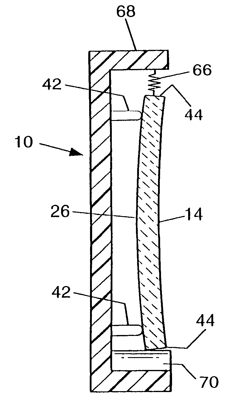
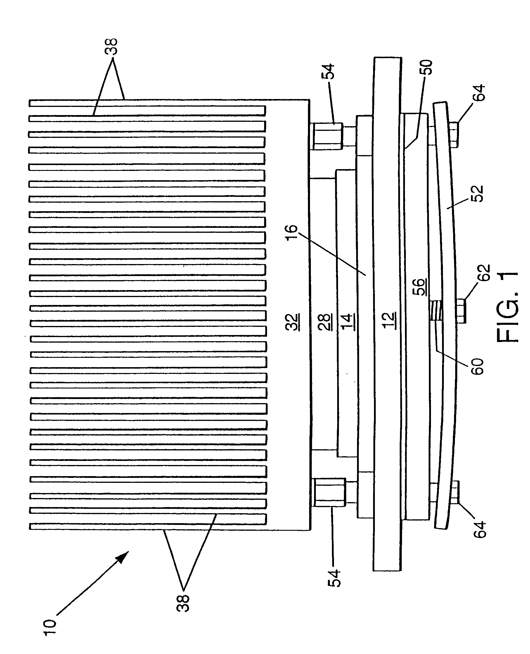
[0040]Referring now to the drawings, and particularly to FIG. 1, an electronic circuit board assembly 10 is shown. The electronic assembly 10 comprises a printed circuit board 12 of standard construction typically composed of multiple circuitized conductive layers interleaved with layers of high dielectric material (these various layers not being shown) in the form of a laminate. One side of the board is backed with an insulator 50 and a stiffener 56. A spring plate 52 is mounted on posts 54 and includes a screw 60 that urges the stiffener against the insulator and the PCB 12, thereby serving to maintain the planarity of the PCB. The screw typically includes an Allen head 62 which is turned with an Allen-head wrench. Turning the screw 60 in one direction increases the spacing between the middle of the spring plate and the stiffener, thereby increasing the pressure exerted by the spring plate on the stiffener at the posts 54. Turning the screw 60 the other way decreases this spacing ...


PUM

PropertyMeasurementUnit
flatnessaaaaaaaaaa
flatnessaaaaaaaaaa
heightaaaaaaaaaa

Abstract

An electronic subassembly comprises a printed circuit board and an electronic module, particularly a ceramic module, electrically connected to one another through a planar interposer. The interposer comprises an insulator sheet and electrical spring elements joining contact sites on the module with contact pads on the PCB. The invention includes modifications that improve the integrity of electrical connections between the printed circuit board and the electronic module. This is achieved by compensating for non-planarity between the surfaces of the interposer and the module, particularly resulting from a convex curvature of the module, by minimizing relative movement, such as rocking in the x-z and y-z planes. It also includes modifications to the suspension of the module within the interposer housing to reduce the effects caused by any sliding that may occur between the interposer and the module in the x-y plane.

Description

CROSS REFERENCE TO RELATED APPLICATIONS[0001]This application is a divisional of application Ser. No. 10 / 059,985, filed Jan. 29, 2002, now U.S. Pat. No. 6,658,729, which in turn is a division of applicaton Ser. No. 09 / 800,148, filed Mar. 6, 2001, now U.S. Pat. No. 6,375,475 B1.FIELD OF THE INVENTION[0002]This invention relates to electrical contacts between printed circuit boards and electronic modules, particularly involving contact sites through land grid array (LGA) sockets.BACKGROUND OF THE INVENTION[0003]A typical LGA interposer system comprises a printed circuit board (PCB) with electrically conductive contact pads, a module (or other printed circuit board) with a corresponding set of electrically conductive contact sites, an interposer between the module and the printed circuit board and an array of spring elements to make electrical contact between the module and the printed circuit board. Clamps are used to mechanically hold the module to the interposer and to electrically ...

Claims


Application Information

Patent Timeline
Patent Type & Authority Patents(United States)
IPC IPC(8): H01R12/00H01R12/71H01R33/76H01R33/975H05K3/32
CPCH01L23/4006H01R13/6315H01R33/7664H01R33/975H05K3/325H01R12/714H01L23/562Y10T29/49126H01L2023/405H01L2023/4062H01L2023/4081H05K2201/10378H05K2201/10719H01L2224/72Y10T29/49117Y10T29/4913
Inventor BRODSKY, WILLIAM LOUIS
Owner IBM CORP
Why Eureka
Try Eureka