
Circuit and method for reducing noise interference in digital differential input receivers

Inactive Publication Date: 2006-01-17
MICRON TECH INC
View PDF3 Cites 5 Cited by
  • Summary
  • Abstract
  • Description
  • Claims
  • Application Information

AI Technical Summary

Benefits of technology

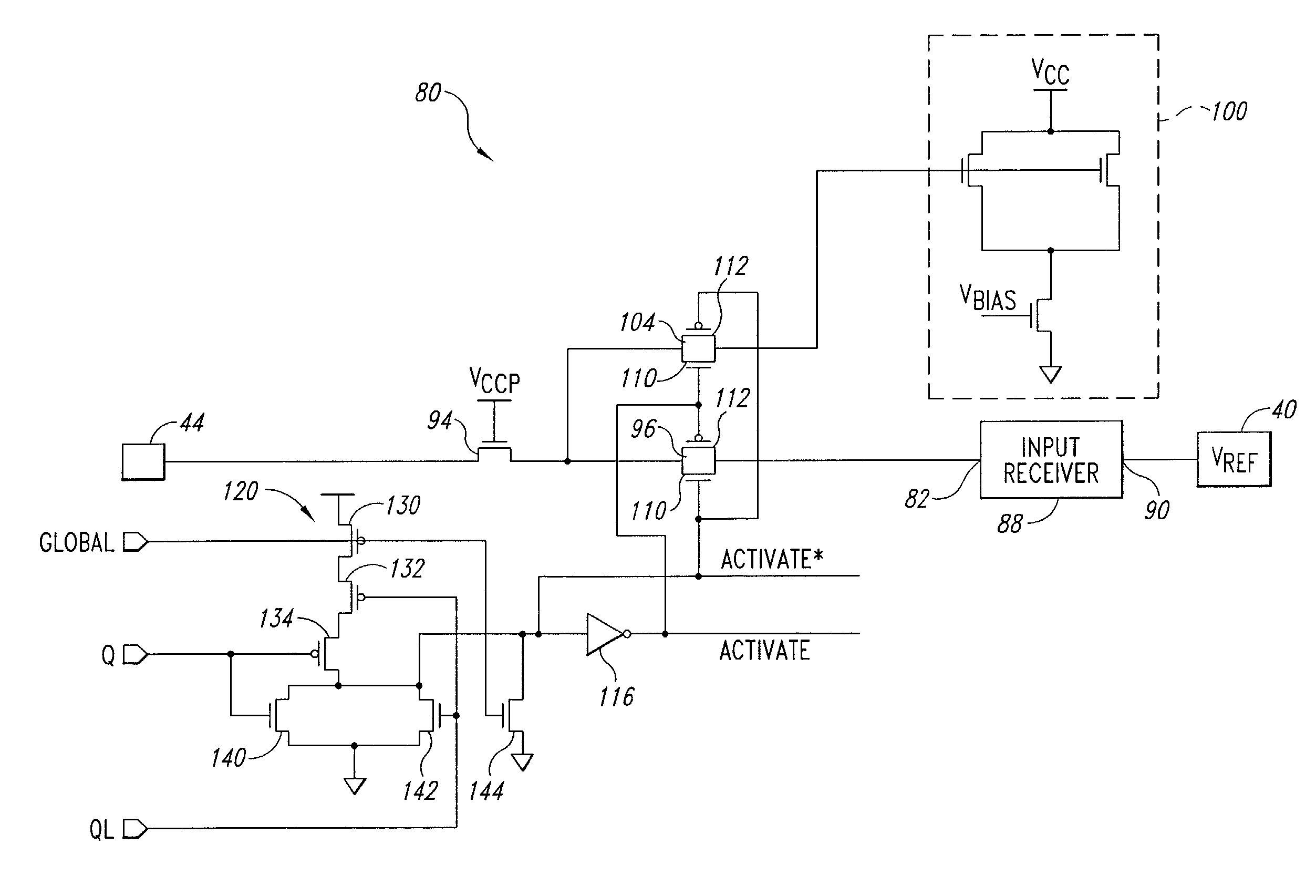
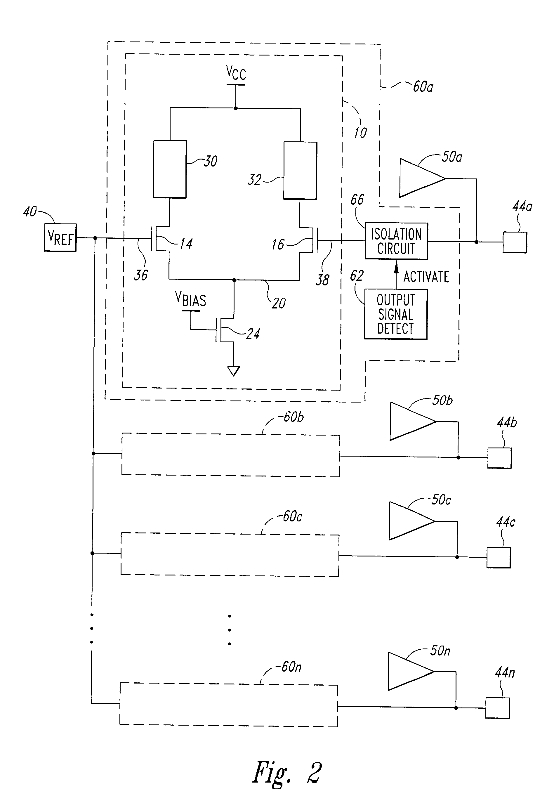
[0009]The present invention is a method and circuit for protecting a reference voltage source from noise generated by applying an output signal to an input/output terminal. The input/output terminal is also coupled to an input receiver that is also coupled to the reference voltage source so that the input receiver can serve as a conduit for coupling transitions of the output signal to the reference voltage source. An output signal detector detects when the output signal is being applied to the input/output terminal. An isolation circuit responds to the output signal being detected by isolating the reference voltage source from the input/output terminal to which the output

Problems solved by technology

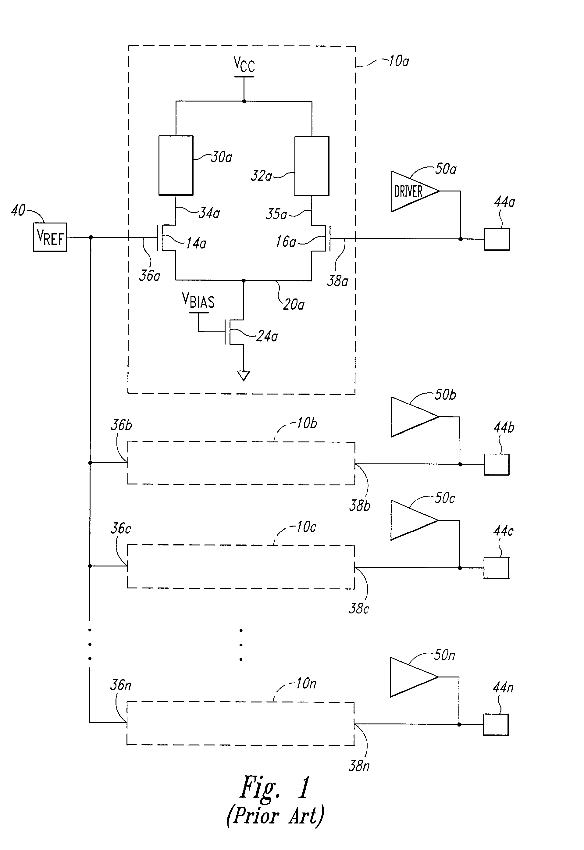
One problem that is often encountered with the input receiver 10 of FIG. 1 results from noise signals present in the reference voltage.
. . n with its own dedicated reference voltage source 40, but doing so might significantly increase the size and cost of integrated circuits using such input receivers 10 because of the large number of terminals 44 typically provided for many integrated circuits.

Method used


Image

  • Circuit and method for reducing noise interference in digital differential input receivers
  • Circuit and method for reducing noise interference in digital differential input receivers
  • Circuit and method for reducing noise interference in digital differential input receivers

Examples


Embodiment Construction

[0017]One embodiment of a circuit that is capable of making the input receiver 10 more immune to noise signals is shown in FIG. 2 in which components common to FIGS. 1 and 2 have been provided with the same reference numerals. In addition to the components of the input receiver 10 shown in FIG. 1, each input receiver circuit 60 in the embodiment of FIG. 2 includes an output signal detector 62 that detects when its respective output driver 50 is applying an output signal to its respective terminal 44. The output signal detector 62 then generates an ACTIVATE signal that is applied to an isolation circuit 66 coupled between the terminal 44 and the second input terminal 38. Although the input receiver circuit 60 shown in FIG. 2 uses an input receiver 10 of the type shown in FIG. 1 in which the second input terminal 38 is coupled to the gate of the transistor 16, other designs for an input receiver may be used.

[0018]The output signal detector 62 may perform its function using a variety o...


PUM


Abstract

A circuit and method reduces noise signals coupled to a reference voltage used by a digital differential input receiver having an input that is coupled to an input / output terminal. The circuit and method selectively isolates the reference voltage from the input / output terminal to which output signals are selectively applied. The isolation occurs responsive to detecting that an output signal is being applied to the input / output terminal so that transitions of the output signal are not coupled through the input receiver to generate noise in the reference voltage. In one embodiment, the isolation is provided by placing an isolation circuit between the input receiver and either the input / output terminal or a source of the reference voltage. In another embodiment, the isolation is provided by selectively biasing the input receiver so that coupling of output signal transitions through the input receiver is substantially reduced.

Description

TECHNICAL FIELD[0001]This invention relates to digital differential input circuits for memory devices and other electronic devices, and, more particularly, to a method and circuit that makes such circuits relatively immune to noise.BACKGROUND OF THE INVENTION[0002]Digital electronic devices, such as memory devices, communicate with external circuitry through input terminals, output terminals, and input / output terminals. These input / output terminals are bi-directional, i.e., digital input signals may be applied to the same terminal to which digital output signals are applied, although not at the same time. One type of input circuit to which input signals are initially applied is a digital differential receiver 10a, an example of which is shown in FIG. 1. The differential receiver 10a includes a pair of NMOS transistors 14, 16 having their sources coupled to a common node 20. The common node 20 is, in turn, coupled to ground through a NMOS current sink transistor 24 that is biased ON ...

Claims


Application Information

Patent Timeline
IPC IPC(8): H04L27/06G11C7/10
CPCG11C7/1084G11C7/1078
Inventor HUBER, BRIAN W.
Owner MICRON TECH INC
Learn More