Method of fabrication of stacked semiconductor devices

a technology of semiconductor devices and fabrication methods, applied in semiconductor devices, semiconductor/solid-state device details, electrical apparatus, etc., can solve the problems of economic undesirable effects of proceeding at less than wafer level, and achieve the effect of increasing the density of semiconductor devices

Inactive Publication Date: 2006-01-24
ROUND ROCK RES LLC
View PDF53 Cites 114 Cited by
  • Summary
  • Abstract
  • Description
  • Claims
  • Application Information

AI Technical Summary

Benefits of technology

[0029]Once the wafers are aligned and adhered, the wafer stack is mounted onto a stretchable adhesive film carried by a frame, as known in the art. The adhesive film is used to immobilize the wafer stack for scribing or sawing to singulate the dice or excise portions or segments of the wafers, sawing being highly preferred over scribing due to the double thickness of the wafer stack. The wafer stack / film frame assembly is then sent through a dicing or singulation procedure wherein individual stacked dice pairs or wafer portions containing groups of dice pairs are cut from the wafer stack using a wafer dicing saw. The “streets” of the front and back wafers of the stack are, of course, aligned such that the circuitry on both wafers is not damaged during the dicing process.
[0032]An upper die of the dice pair can be used to align the dice pair to the substrate. The use of the upper die for alignment allows the dice pair to be placed within plus or minus 0.0002–0.0003 inch of the desired location. Optical alignment systems including, without limitation, pattern recognition systems as known in the art, are suitable to effect alignment to such tolerances. Once the dice pair is attached, an under-fill encapsulant is generally disposed between the lower die and the substrate (if other than a leadframe) for environmental protection and to enhance the attachment of the dice pair to the substrate.

Problems solved by technology

It is, of course, understood that the above alignment, adherence and separation process can be employed using portions of wafers rather than full wafers, although this is not preferred and may be impractical since handling and sawing equipment is generally designed to accommodate full wafers, and proceeding at less than wafer level may be economically undesirable.

Method used


Image

  • Method of fabrication of stacked semiconductor devices
  • Method of fabrication of stacked semiconductor devices
  • Method of fabrication of stacked semiconductor devices

Examples


Embodiment Construction

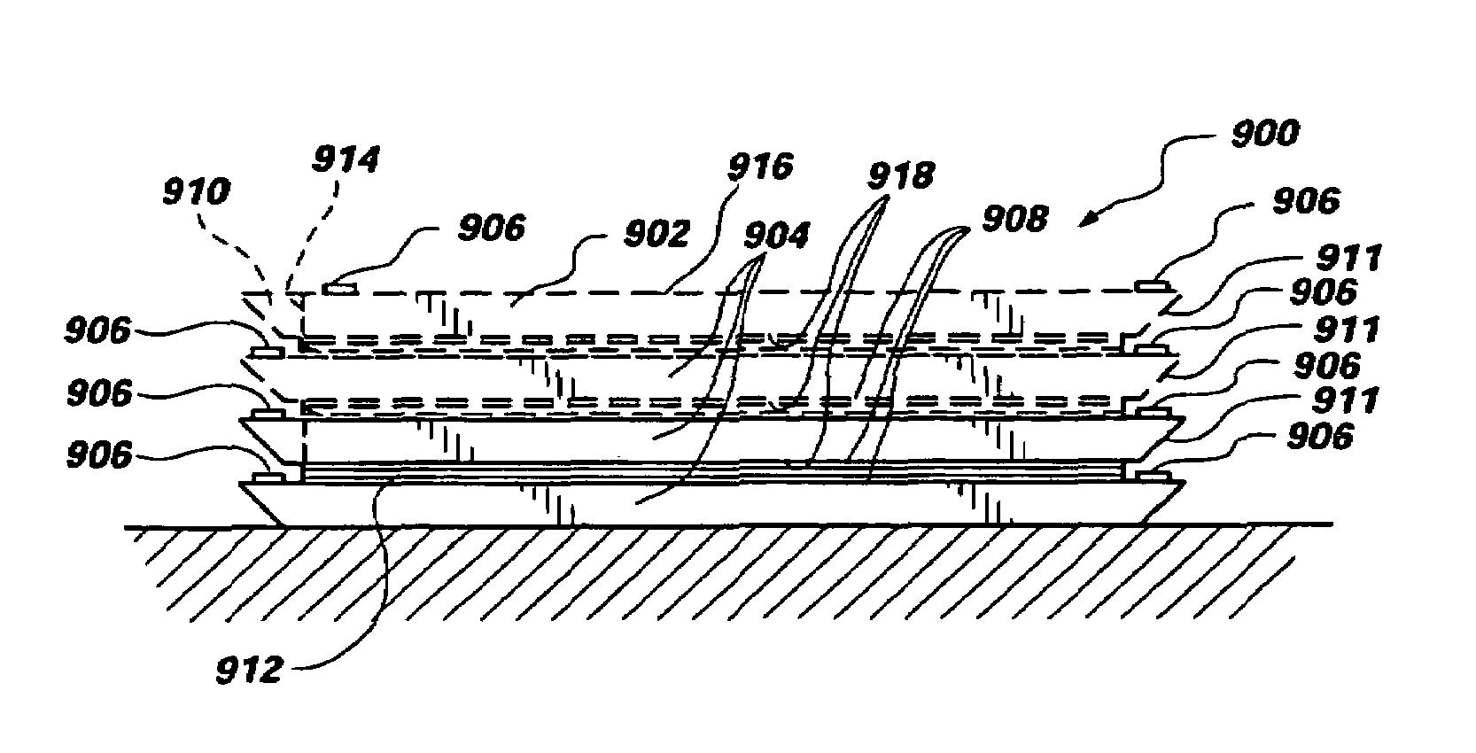
[0048]FIG. 1 illustrates a top plan view of an exemplary completed wafer 100 of the present invention. The wafer 100 comprises an upper surface 102 displaying the active sides of a plurality of dice 104. The dice 104 each contain identical integrated circuitry, which will be independently functional after the dice 104 are separated from the wafer 100. While in practice, the dice 104 are extremely closely packed on the wafer 100 and essentially contiguous, but for the wafer material sacrificed during sawing, the dice 104 have been shown as more widely spaced for clarity in disclosure of the method of the invention. The wafer 100 also includes a flat lateral edge 106, as known in the art. The method of the present invention comprises fabricating appropriate circuitry in the upper wafer surface 102 at the locations of the dice 104 by techniques well known in the industry.

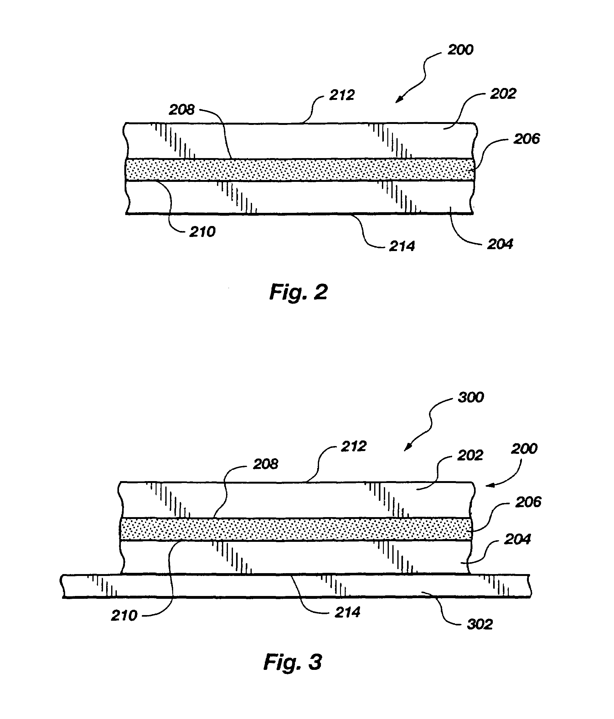
[0049]As shown in FIG. 2, a wafer pair assembly 200 comprises completed wafers 202 (upper wafer) and 204 (lower wafe...


PUM


Abstract

A method for increasing integrated circuit density is disclosed comprising stacking an upper wafer and a lower wafer, each of which having fabricated circuitry in specific areas on their respective face surfaces. The upper wafer is attached back-to-back with the lower wafer with a layer of adhesive applied over the back side of the lower wafer. The wafers are aligned so as to bring complementary circuitry on each of the wafers into perpendicular alignment. The adhered wafer pair is then itself attached to an adhesive film to immobilize the wafer during dicing. The adhered wafer pair may be diced into individual die pairs or wafer portions containing more than one die pair.

Description

CROSS-REFERENCE TO RELATED APPLICATIONS[0001]This application is a divisional of application Ser. No. 09 / 943,880, filed Aug. 30, 2001, now U.S. Pat. No. 6,784,023, issued Aug. 31, 2004, which is a continuation of application Ser. No. 09 / 651,394, filed Aug. 29, 2000, now U.S. Pat. No. 6,337,227, issued Jan. 8, 2002, which is a continuation of application Ser. No. 08 / 844,669 filed Apr. 18, 1997, now U.S. Pat. No. 6,165,815, issued Dec. 26, 2000, which is a continuation of application Ser. No. 08 / 650,429, filed May 20, 1996, abandoned.BACKGROUND OF THE INVENTION[0002]1. Field of the Invention[0003]The present invention relates to an apparatus and a method for increasing semiconductor device density. In particular, the present invention relates to a method for producing vertically superimposed multi-chip devices usable with combined flip-chip, wire bond, and / or tape automated bonding (“TAB”) assembly techniques to achieve densely packaged semiconductor devices.[0004]2. State of the Art[...

Claims


Application Information

Patent Timeline
Patent Type & Authority Patents(United States)
IPC IPC(8): H01L21/00H01L23/48H01L21/98H01L25/065H01L29/06
CPCH01L21/6836H01L24/27H01L25/0657H01L25/50H01L29/0657H01L2221/68327H01L2224/16225H01L2224/274H01L2224/45124H01L2224/45144H01L2224/48091H01L2224/48227H01L2224/73265H01L2225/0651H01L2225/06517H01L2225/06551H01L2225/06555H01L2225/06589H01L2924/01079H01L2924/14H01L24/45H01L2924/01013H01L2224/32225H01L2224/32145H01L2224/73253H01L2224/73204H01L2924/00014H01L2924/00H01L2924/3512H01L2924/00012H01L24/73H01L2224/05568H01L2224/05573H01L2924/181H01L2224/05599
Inventor BALL, MICHAEL B.
Owner ROUND ROCK RES LLC
Why Eureka
Try Eureka