Semiconductor device having a bond pad and method therefor

Inactive Publication Date: 2005-01-18
SK HYNIX INC
View PDF11 Cites 160 Cited by
  • Summary
  • Abstract
  • Description
  • Claims
  • Application Information

AI Technical Summary

Problems solved by technology

One problem with using a mechanical interface, for example, a probe needle, is that the bond pads may be damaged or contaminated, preventing a reliable electrical connection between the bond pad and the package pin when the die is wire bonded.
This problem is made worse by the decreasing bond pad geometries characteristic of modern deep

Method used


Image

  • Semiconductor device having a bond pad and method therefor
  • Semiconductor device having a bond pad and method therefor
  • Semiconductor device having a bond pad and method therefor

Examples


Example

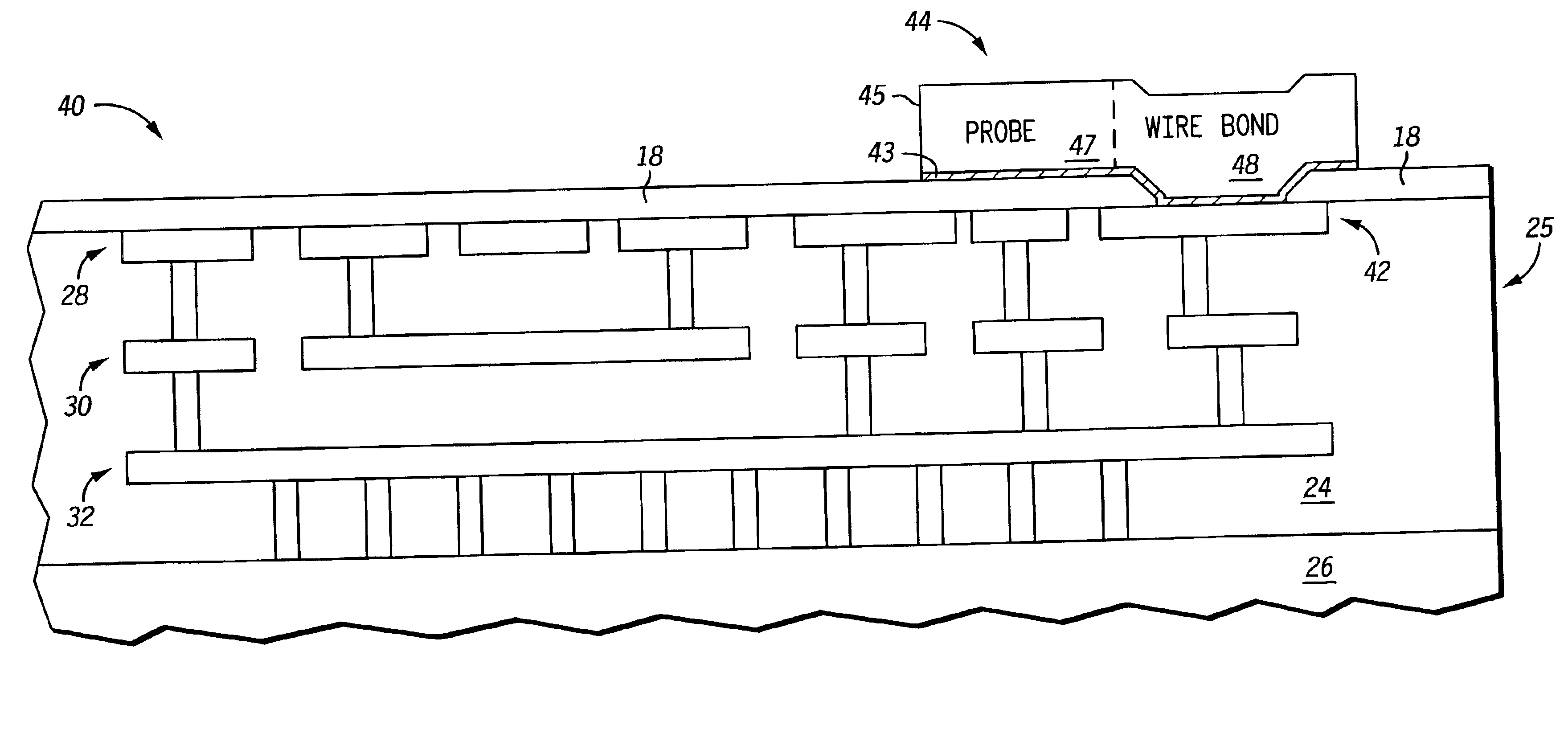
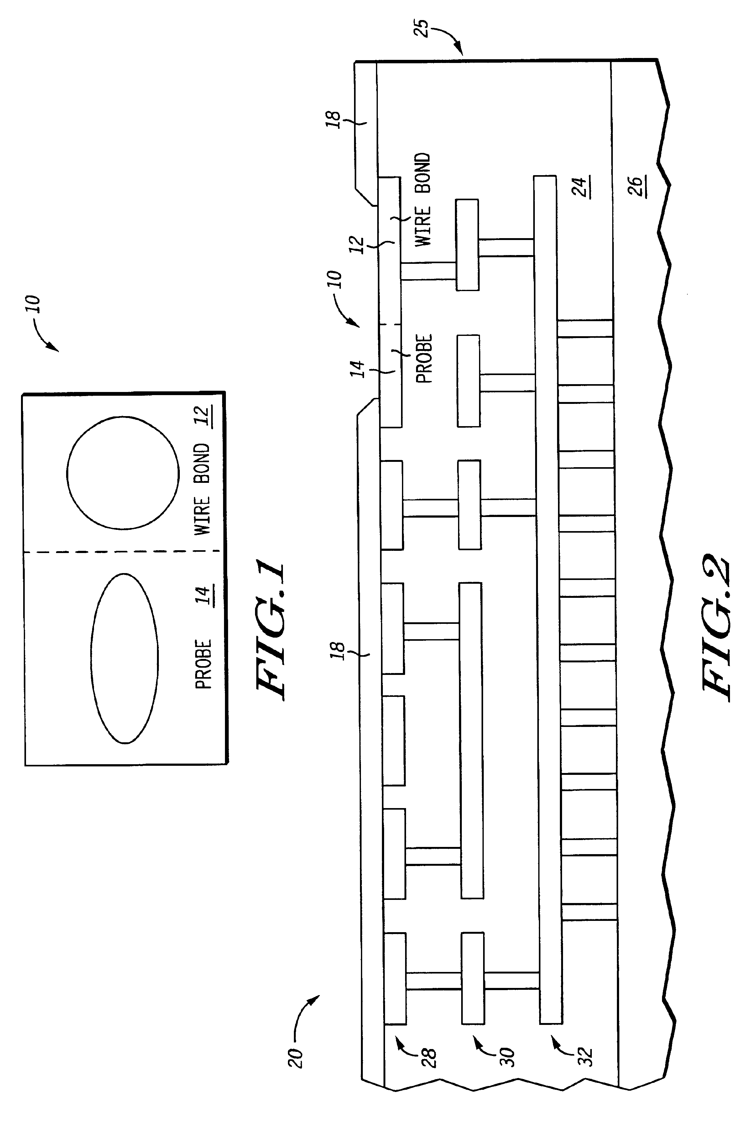
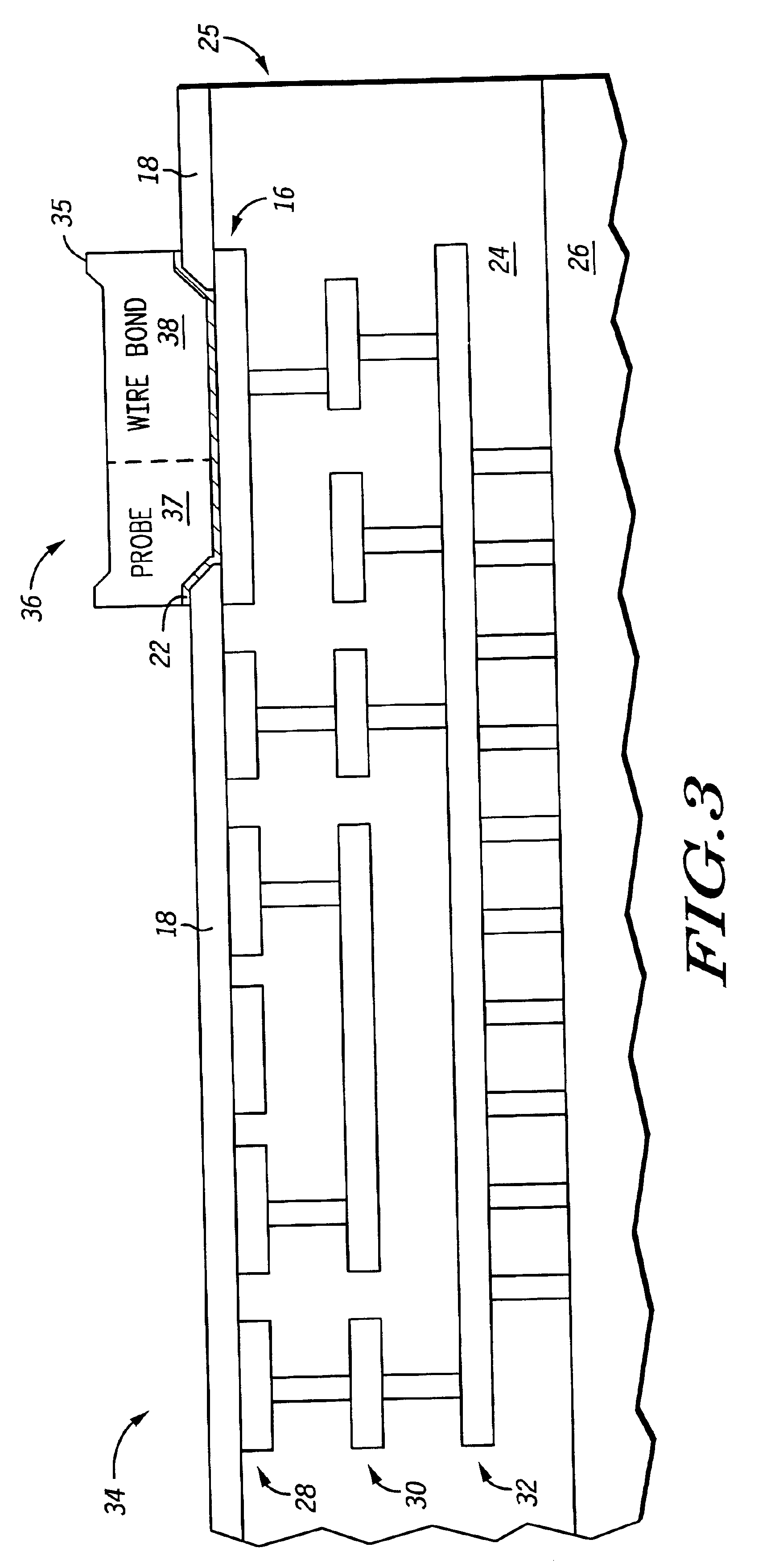
Generally, the present invention provides an integrated circuit having a plurality of bond pads. Each of the plurality of bond pads has a probe region and a wire bond region that are substantially non-overlapping and contiguous. In one embodiment, a bond pad extends over active circuitry and / or electrical interconnect layers of the integrated circuit. A portion of, or all, of the bond pad extends over the interconnect layers and a portion of the pad may be formed over a passivation layer and connected to a final metal layer pad. In one embodiment, the bond pad is formed from aluminum and the final metal layer pad is formed from copper.

Separating the probe region from the wire bond region and forming the bond pad over active circuitry has several advantages. In an application requiring very fine pitch between the bond pads, the probe regions and active regions may be staggered to effectively increase the distance between probe regions. By separating the probe region from the wire bon...


PUM


Abstract

A bond pad (10) has a probe region (14) and a wire bond region (12) that are substantially non-overlapping. In one embodiment, the bond pad (10) is connected to a final metal layer pad (16) and extends over an interconnect region (24). The bond pad (10) is formed from aluminum and the final metal layer pad (16) is formed from copper. Separating the probe region (14) from the wire bond region (12) prevents the final metal layer pad (16) from being damaged by probe testing, allowing for more reliable wire bonds. In an application requiring very fine pitch between bond pads, the probe regions (14) and active regions (12) of a plurality of bond pads formed in a line may be staggered to increase the distance between the probe regions (14). In addition, forming the bond pads (10) over the interconnect region (24) reduces the size of the integrated circuit.

Description

FIELD OF THE INVENTIONThe present invention relates generally to semiconductor devices, and more particularly, to a semiconductor device having a bond pad for probe and wire bond isolation and method therefor.BACKGROUND OF THE INVENTIONIn integrated circuit manufacturing, wire bonding is a well proven method used to connect a semiconductor die having electrical circuitry to a pin on a component package. Within integrated circuit manufacturing it is also a common practice to test the functionality of the semiconductor die before completing component assembly. “Probe test” is one such method used to test a semiconductor where a probe contact is commonly used as a mechanical and electrical interface to bond pads on the die.One problem with using a mechanical interface, for example, a probe needle, is that the bond pads may be damaged or contaminated, preventing a reliable electrical connection between the bond pad and the package pin when the die is wire bonded. This problem is made wo...

Claims


Application Information

Patent Timeline
IPC IPC(8): H01L23/58H01L23/48H01L23/485H01L21/60H01L21/66
CPCH01L22/32H01L24/05H01L24/03H01L2224/02166H01L2224/05073H01L2224/05166H01L2224/05187H01L2224/05553H01L2224/05624H01L2224/48145H01L2225/06506H01L2225/0651H01L2225/06596H01L2924/01004H01L2924/01013H01L2924/01014H01L2924/01022H01L2924/01028H01L2924/01029H01L2924/01033H01L2924/01073H01L2924/01074H01L2924/01079H01L2924/01082H01L2924/04941H01L2924/04953H01L2924/05042H01L2924/14H01L2224/04042H01L2924/01006H01L2924/00014H01L2924/00H01L2224/0392H01L2224/023H01L2924/00012H01L2924/0001
Inventor YONG, LOIS E.HARPER, PETER R.TRAN, TU ANHMETZ, JEFFREY W.LEAL, GEORGE R.DINH, DIEU VAN
Owner SK HYNIX INC
Why Eureka
Try Eureka