Bitline implant utilizing dual poly

a technology of dual polymer and bitline, applied in the field of memory for computer systems, can solve the problems of reducing data storage density affecting the performance of the device, etc., and achieving the effect of improving vt roll-off, saving resources and space, and less energy

Active Publication Date: 2006-01-24
INFINEON TECH LLC
View PDF24 Cites 6 Cited by
  • Summary
  • Abstract
  • Description
  • Claims
  • Application Information

AI Technical Summary

Benefits of technology

[0019]The present invention pertains to implementing a dual poly process in forming a transistor based memory device. The process allows buried bitlines to be formed with less energy and to shallower depths than conventional bitlines to save resources and space, and to improve Vt roll-off. Oxide materials are also formed over the buried bitlines to improve (e.g., increase) a breakdown voltage between the bitlines and wordlines, thus allowing for greater discrimination between programming and erasing charges and more reliable data storage. The process also facilitates a reduction in buried bitline width and thus allows bitlines to be formed closer together. As a result, more devices can be “packed” within the same or a smaller area.

Problems solved by technology

For example, DRAM and SRAM allow individual bits of data to be erased one at a time, but such memory loses its data when power is removed.
EEPROM can alternatively be easily erased without extra exterior equipment, but has reduced data storage density, lower speed, and higher cost.
This could result in corrupt data and / or inaccurately stored or programmed data.
Similarly, other issues, such as leakage currents, cross talk, etc. can also result from scaling.
For example, isolating two bits or charges stored in a charge trapping layer becomes increasingly difficult as the channel length is decreased and the bits are brought closer together.

Method used


Image

  • Bitline implant utilizing dual poly
  • Bitline implant utilizing dual poly
  • Bitline implant utilizing dual poly

Examples


Embodiment Construction

[0030]One or more aspects of the present invention are described with reference to the drawings, wherein like reference numerals are generally utilized to refer to like elements throughout, and wherein the various structures are not necessarily drawn to scale. In the following description, for purposes of explanation, numerous specific details are set forth in order to provide a thorough understanding of one or more aspects of the present invention. It may be evident, however, to one skilled in the art that one or more aspects of the present invention may be practiced with a lesser degree of these specific details. In other instances, well-known structures and devices are shown in block diagram or other form in order to facilitate describing one or more aspects of the present invention.

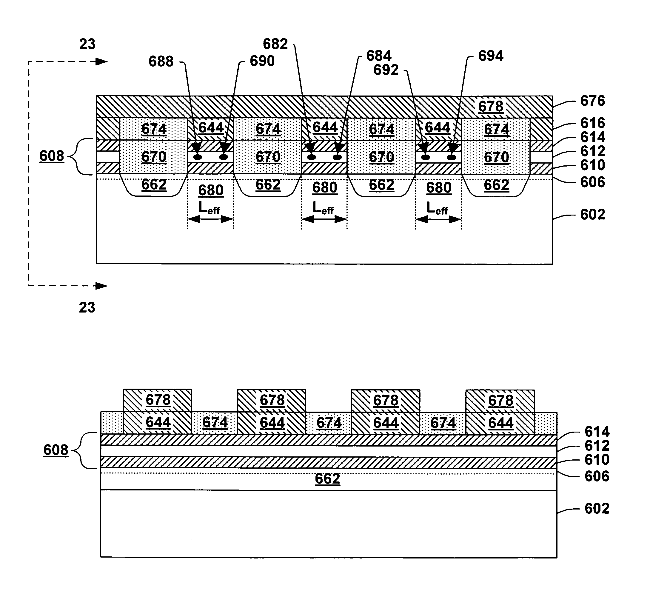
[0031]The present invention pertains to implementing a dual poly process in forming a transistor based memory device. The process allows buried bitlines to be formed with less energy and to shallower ...


PUM


Abstract

The present invention pertains to implementing a dual poly process in forming a transistor based memory device. The process allows buried bitlines to be formed with less energy and to shallower depths than conventional bitlines to save resources and space, and to improve Vt roll-off. Oxide materials are also formed over the buried bitlines to improve (e.g., increase) a breakdown voltage between the bitlines and wordlines, thus allowing for greater discrimination between programming and erasing charges and more reliable resulting data storage. The process also facilitates a reduction in buried bitline width and thus allows bitlines to be formed closer together. As a result, more devices can be “packed” within the same or a smaller area.

Description

RELATED APPLICATIONS[0001]This application is related to U.S. patent application Ser. No. 10 / 755,430, filed on Jan. 12, 2004, entitled “NARROW BITLINE USING SAFIER FOR MIRROR BIT”, U.S. patent application Ser. No. 10 / 729,732, filed on Dec. 5, 2003, entitled “HARD MASK SPACER FOR SUBLITHOGRAPHIC BITLINE”, U.S. patent application Ser. No. 10 / 755,740, filed on Jan. 12, 2004, entitled POCKET IMPLANT FOR COMPLEMENTARY BIT DISTURB IMPROVEMENT AND CHARGING IMPROVEMENT OF SONOS MEMORY CELL” and U.S. patent application Ser. No. 10 / 862,636, filed on Jun. 7, 2004, entitled “LDC IMPLANT FOR MIRRORBIT TO IMPROVE Vt ROLL-OFF AND FORM SHARPER JUNCTION”.FIELD OF INVENTION[0002]The present invention relates generally to memory for computer systems and the like, and in particular to implementing a dual poly process that assists in allowing relatively shallow implanted bitlines to be formed.BACKGROUND OF THE INVENTION[0003]Many different types and styles of memory exist to store data for computers and...

Claims


Application Information

Patent Timeline
Patent Type & Authority Patents(United States)
IPC IPC(8): H01L21/425H01L21/8246H01L27/115
CPCH01L27/11568H01L27/115H10B69/00H10B43/30B82Y10/00H10B99/00
Inventor QIAN, WEIDONGRAMSBEY, MARKYANG, JEAN YEE-MEIHADDAD, SAMEER
Owner INFINEON TECH LLC
Why Eureka
Try Eureka