Die-up ball grid array package with patterned stiffener opening

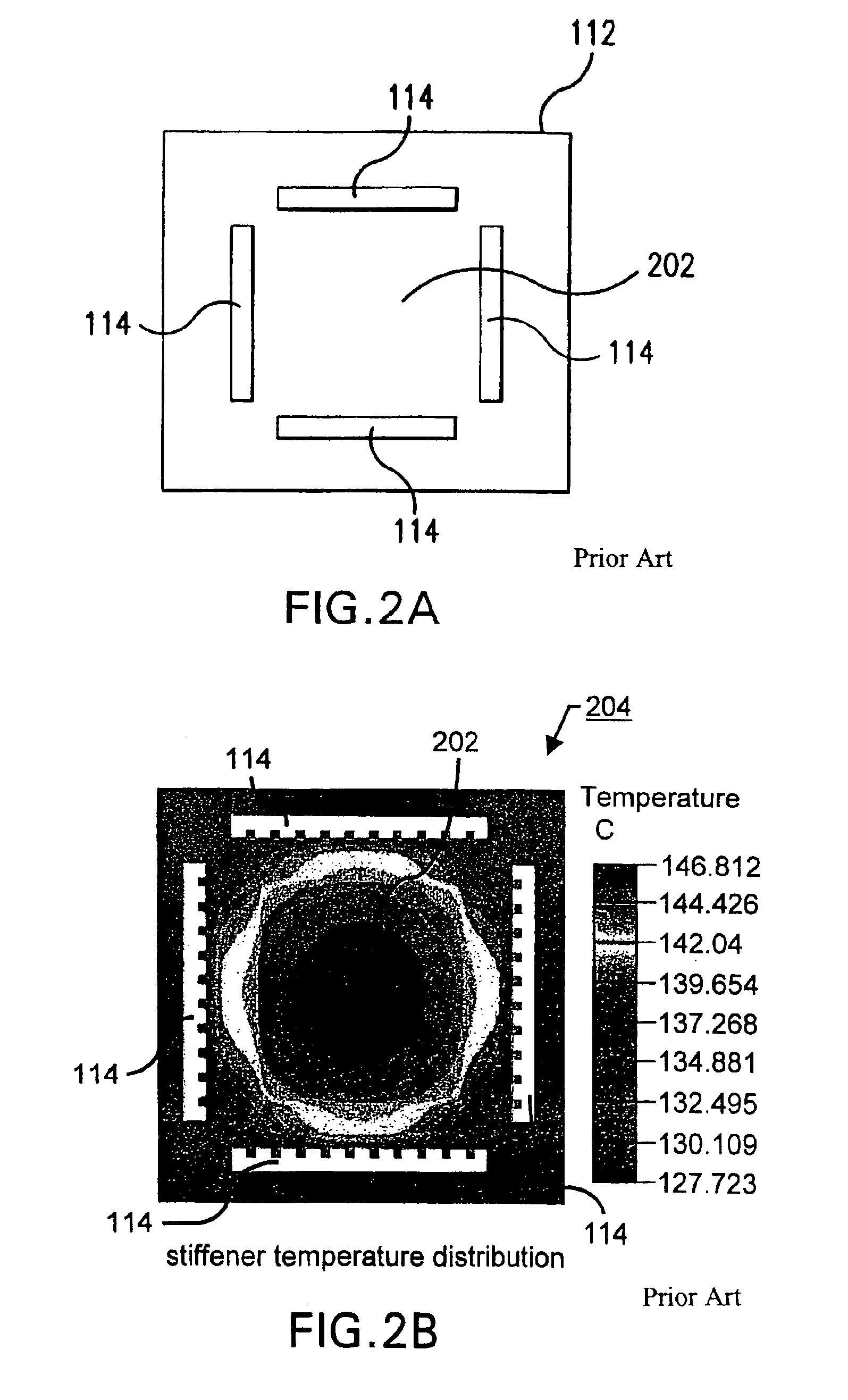
a grid array package and patterned stiffener technology, applied in the direction of semiconductor devices, semiconductor/solid-state device details, electrical equipment, etc., can solve the problems of reducing the thermal connection between the ic die and the edge of the stiffener, reducing the reliability requirements of die sizes larger than 9 mm, and high thermal stress of conventional bga packages

Inactive Publication Date: 2006-01-24
AVAGO TECH INT SALES PTE LTD
View PDF148 Cites 91 Cited by
  • Summary
  • Abstract
  • Description
  • Claims
  • Application Information

AI Technical Summary

Problems solved by technology

Conventional BGA packages are subject to high thermal stresses that result from the heat given off during operation of the mounted IC die.
As a result, conventional flex BGA packages have difficulty in meeting reliability requirements for die sizes larger than 9 mm.
However, the openings on the stiffener for wire bond connections tend to reduce the thermal connections between the IC die and the edges of the stiffener.
As a result, heat spreading is limited largely to the region of the IC die attach pad, while areas at the stiffener peripheral do not contribute effectively to heat spreading.
Furthermore, because of the high density of the substrate routing circuitry, it is difficult to bond each power and ground pad on the IC die to the substrate by a corresponding bond finger.
As a result, the distribution of ground and power signals connecting to the IC die is frequently compromised in conventional BGA packages.
The cost of the PBGA package, however, will increase with the number of thermal balls.
Furthermore, a large array of thermal balls may be necessary for heat dissipation into the PCB for high levels of IC device power.

Method used


Image

  • Die-up ball grid array package with patterned stiffener opening
  • Die-up ball grid array package with patterned stiffener opening
  • Die-up ball grid array package with patterned stiffener opening

Examples


Embodiment Construction

Overview

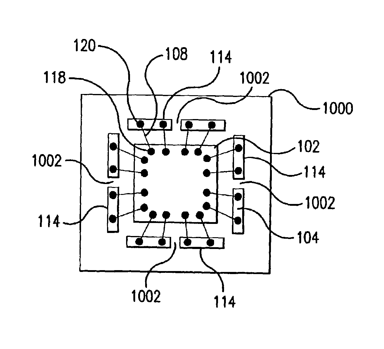
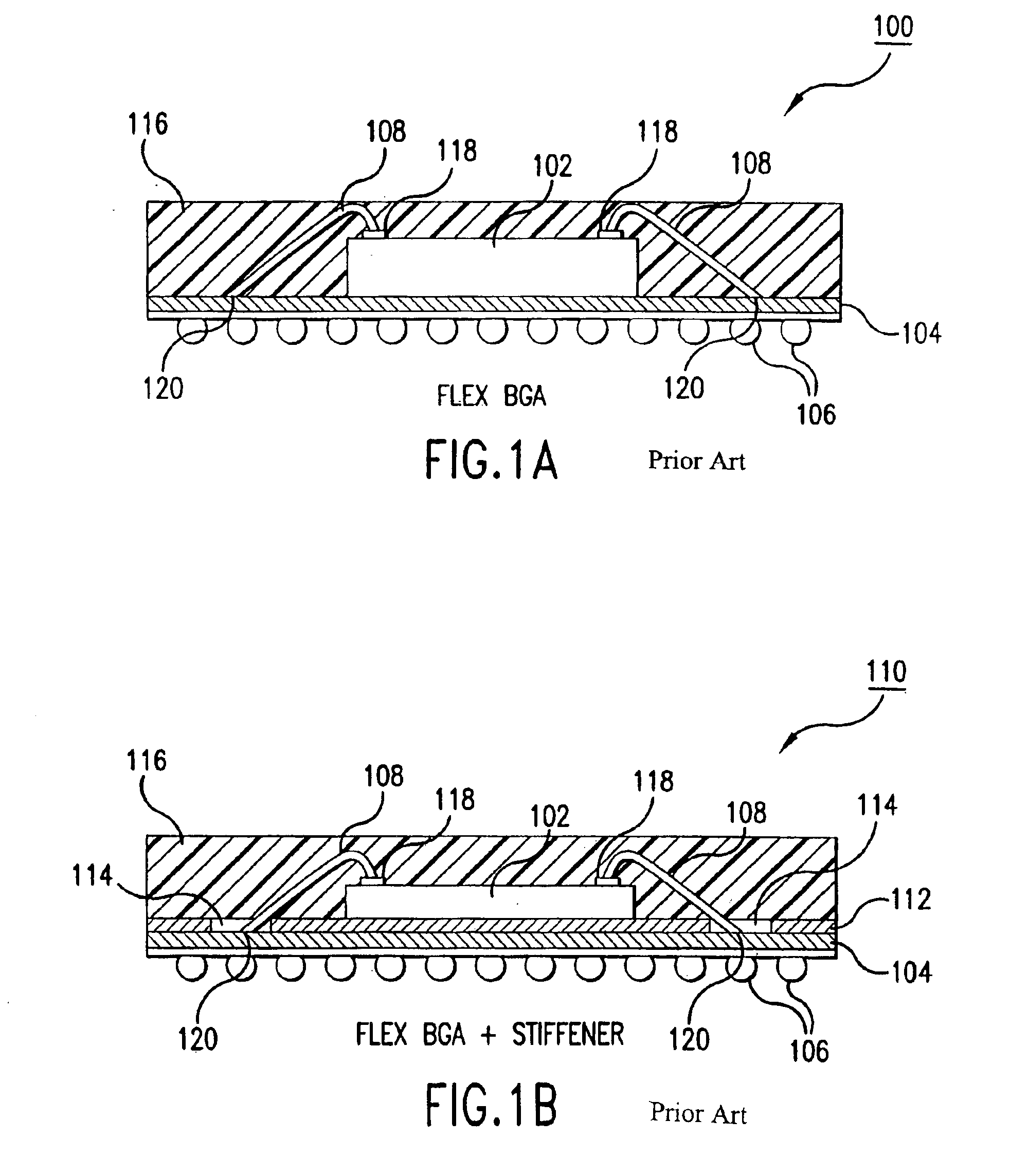
[0050]The present invention is directed to a method and system for improving the mechanical, thermal, and electrical performance of BGA packages. The present invention is applicable to all types of BGA substrates, including ceramic, plastic, and tape (flex) BGA packages. Furthermore the present invention is applicable to die-up (cavity-up) and die-down (cavity-down) orientations.

[0051]Numerous embodiments of the present invention are presented herein. In a first embodiment, BGA package thermal stress at the IC die / stiffener interface is released or altered with the introduction of a heat spreader on the top surface of the IC die, enabling large size dies with high input and output (I / O) counts to be packaged using BGA technology. In a second embodiment, BGA package thermal resistance and the length of the current return path are reduced by introducing thermal / ground balls underneath or within close proximity of the IC die. In a third embodiment, the package thermal resistanc...


PUM


Abstract

An electrically and thermally enhanced die-up tape substrate ball grid array (BGA) package and die-up plastic substrate BGA package are described. A substrate that has a first surface and a second surface is provided. The stiffener has a first surface and a second surface. The second stiffener surface is attached to the first substrate surface. An IC die has a first surface and a second surface. The first IC die surface is mounted to the first stiffener surface. A plurality of solder balls is attached to the second substrate surface. In one aspect, a heat spreader is mounted to the second IC die surface. In another aspect, the stiffener is coupled to ground to act as a ground plane. In another aspect, the substrate has a window opening that exposes a portion of the second stiffener surface. The exposed portion of the second stiffener surface is configured to be coupled to a printed circuit board (PCB). In another aspect, a metal ring is attached to the first stiffener surface. In another aspect, wire bond openings in the stiffener are bridged by one or more studs.

Description

CROSS REFERENCE TO RELATED APPLICATION[0001]This application is a divisional of Application No. 09 / 742,366, filed on Dec. 22, 2000, which is incorporated herein by reference in its entirety.BACKGROUND OF THE INVENTION[0002]1. Field of the Invention[0003]The invention relates generally to the field of integrated circuit (IC) device packaging technology, and more particularly to substrate stiffening and heat spreading techniques in ball grid array (BGA) packages.[0004]2. Related Art[0005]Integrated circuit (IC) dies are typically mounted in or on a package that is attached to a printed circuit board (PCB). One such type of IC die package is a ball grid array (BGA) package. BGA packages provide for smaller footprints than many other package solutions available today. A BGA package has an array of solder balls located on a bottom external surface of a package substrate. The solder balls are reflowed to attach the package to the PCB. The IC die is mounted to a top surface of the package ...

Claims


Application Information

Patent Timeline
Patent Type & Authority Patents(United States)
IPC IPC(8): H01L23/10H01L23/34H01L23/48H01L23/52H01L23/373H01L23/433
CPCH01L23/3677H01L23/4334H01L23/49816H01L23/49838H01L23/50H01L23/562H01L23/3735H01L2224/73265H01L2224/48227H01L2224/48228H01L2224/48237H01L2224/48465H01L2224/49109H01L2224/49171H01L2924/01013H01L2924/01029H01L2924/01039H01L2924/01046H01L2924/01078H01L2924/01079H01L2924/1433H01L2924/15153H01L2924/15165H01L2924/15311H01L2924/19041H01L2924/30107H01L24/48H01L24/49H01L2224/32225H01L2224/73215H01L2924/00H01L2924/00012H01L2924/351H01L2924/15787H01L2924/181H01L2224/45144H01L24/45H01L2924/14H01L2224/2929H01L2224/29339H01L2224/32245H01L2224/33181H01L2224/05624H01L2224/8385H01L2924/00014H01L2924/0665H01L23/34H01L23/5384H01L24/14
Inventor KHAN, REZA-UR RAHMANZHAO, SAM ZIQUNBACHER, BRENT
Owner AVAGO TECH INT SALES PTE LTD
Why Eureka
Try Eureka