Column read amplifier power-gating technique for integrated circuit memory devices and those devices incorporating embedded dynamic random access memory (DRAM)

a technology of integrated circuit memory and column read amplifier, which is applied in the direction of information storage, static storage, digital storage, etc., can solve the problems of consuming a large amount of on-chip area, reducing the switching speed of the read amplifier, and unacceptably large current surge through the power-gating transistor, so as to reduce power, reduce the current through the pass transistor, and save the effect of on-chip area

Active Publication Date: 2006-01-24
SONY CORP
View PDF3 Cites 7 Cited by
  • Summary
  • Abstract
  • Description
  • Claims
  • Application Information

AI Technical Summary

Benefits of technology

[0008]Disclosed herein is a column read amplifier power-gating technique for DRAM devices and those devices incorporating embedded DRAM which incorporate a power-down (or Sleep) mode of operation which overcomes the deficiencies of conventional power-gating approaches. It advantageously eliminates the need for a large, separate power-gating transistor thereby saving on-chip area yet still reduces power during Sleep Mode. In operation, instead of adding the additional power-gating device, the column select signal YR is controlled such that it is now driven below VSS during Sleep Mode when N-channel pass transistors are used. If P-channel devices are used, the YR signal is driven above a supply voltage level of VCC. In either case, this significantly reduces the current through the pass transistors and yet causes no reduction in the switching speed of the column read amplifiers.

Problems solved by technology

The difficulty with this approach is that in the Select Mode, the current surge through the power-gating transistor can be unacceptably large due to the fact that multiple read amplifiers switch simultaneously.
This causes a voltage drop across the power-gating transistor which reduces the switching speed of the read amplifiers.
Furthermore, as previously mentioned, the power-gating transistor must be made very large in an attempt to minimize this voltage drop, thereby also consuming a large amount of on-chip area.

Method used


Image

  • Column read amplifier power-gating technique for integrated circuit memory devices and those devices incorporating embedded dynamic random access memory (DRAM)
  • Column read amplifier power-gating technique for integrated circuit memory devices and those devices incorporating embedded dynamic random access memory (DRAM)
  • Column read amplifier power-gating technique for integrated circuit memory devices and those devices incorporating embedded dynamic random access memory (DRAM)

Examples


Embodiment Construction

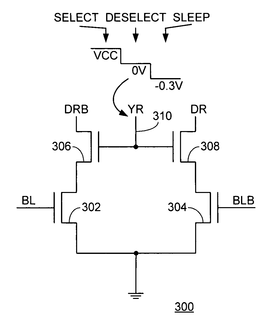
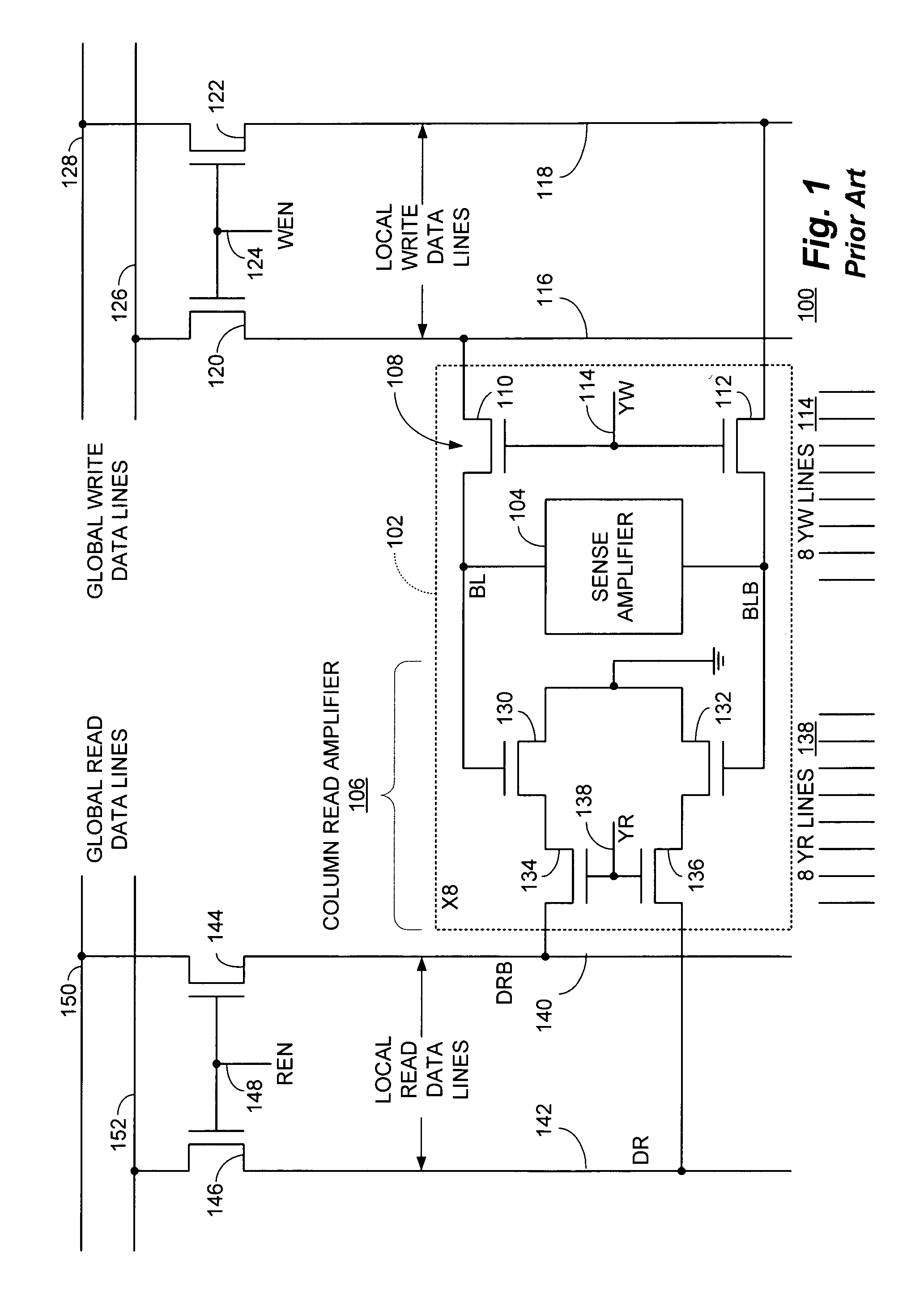
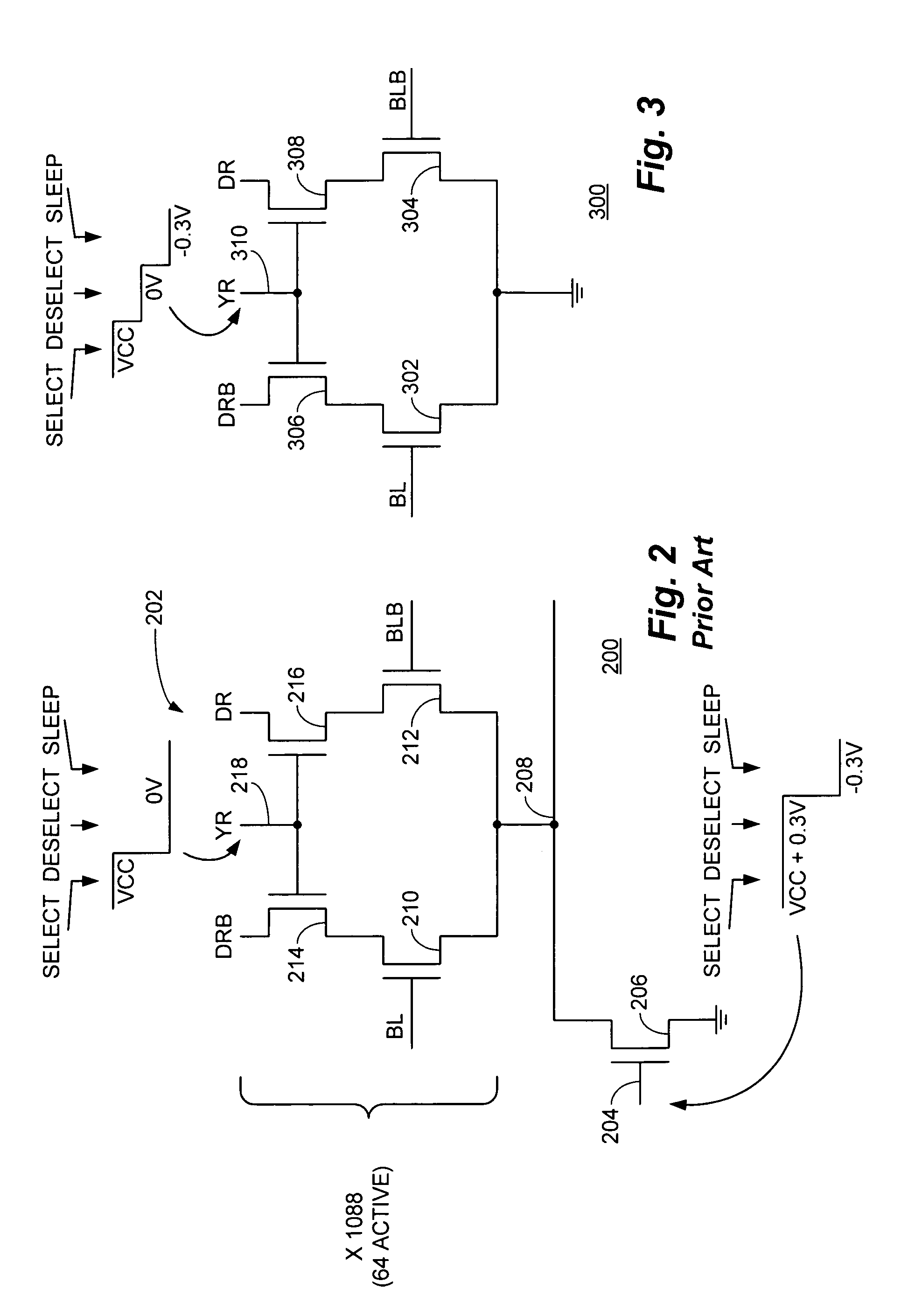
[0013]With reference now to FIG. 1, a high level schematic and functional block diagram of the global and local read and write data lines of a conventional, integrated circuit memory array 100 are shown together with a representative sense amplifier and associated non-power-gated column read and write circuitry.

[0014]The memory array 100 comprises, in pertinent part, a read / write circuit 102 which may, in a particular implementation, comprise one of eight such circuits as indicated. The read / write circuit 102 comprises a sense amplifier 104 coupled between a pair of complementary bit lines (BL and. BLB). Associated with each sense amplifier 104 is a column read amplifier 106 and a column write circuit 108, the former of which will be more fully describe hereinafter.

[0015]Global write data lines 126 and 128 are selectively coupled through N-channel transistors 120 and 122 respectively to local write data lines 116 and 118 in response to a write enable (WEN) signal applied to the gate...


PUM


Abstract

A column read amplifier power-gating technique for DRAM devices and those devices incorporating embedded DRAM which incorporate a power-down (or Sleep) mode of operation which overcomes the deficiencies of conventional power-gating approaches by eliminating the need for a large, separate power-gating transistor thereby saving on-chip area yet still reducing power during Sleep Mode. In operation, the column select signal YR is controlled such that it is driven below VSS during Sleep Mode when N-channel pass transistors are used in the column read amplifier or to a supply voltage level of VCC when P-channel devices are used instead. This significantly reduces the current through the pass transistors and yet causes no reduction in the switching speed of the column read amplifiers.

Description

CROSS REFERENCE TO RELATED PATENT APPLICATIONS[0001]The present invention is related to, and claims priority from, U.S. Provisional Patent Application Ser. No. 60 / 500,126 filed Sep. 4, 2003 for: “0.6V 205 MHz 19.5 nsec TRC 16 Mb Embedded DRAM” the disclosure of which is herein specifically incorporated in its entirety by this reference. The present invention is further related to the subject matter disclosed in U.S. patent applications Ser. No. 10 / 776,103 entitled: “Sense Amplifier Power-Gating Technique for Integrated Circuit Memory Devices and Those Devices Incorporating Embedded Dynamic Random Access Memory (DRAM)” and 10 / 776,101 entitled: “High Speed Power-Gating Technique for Integrated Circuit Devices Incorporating a Sleep Mode of Operation”, the disclosures of which are herein specifically incorporated by this reference in its entirety.BACKGROUND OF THE INVENTION[0002]The present invention relates, in general, to the field of integrated circuit memory devices and those device...

Claims


Application Information

Patent Timeline
Patent Type & Authority Patents(United States)
IPC IPC(8): G11C7/00G11C11/409G11C7/10G11C7/18G11C11/407
CPCG11C7/1048G11C7/18G11C2207/2227G11C2207/002
Inventor HARDEE, KIM C.
Owner SONY CORP
Why Eureka
Try Eureka