Electron-emitting device and image display apparatus using the same

a technology of electron-emitting devices and image display apparatuses, which is applied in the manufacture of electric discharge tubes/lamps, discharge tubes with screens, discharge tubes luminescnet screens, etc., can solve the problems of substrate handling conditions specific to the above production method, drop application conditions, drop forming conditions and substrate handling conditions, etc., to achieve low cost production, easy production of electron-emitting devices, and high accuracy

Inactive Publication Date: 2006-01-31
RICOH KK
View PDF25 Cites 17 Cited by
  • Summary
  • Abstract
  • Description
  • Claims
  • Application Information

AI Technical Summary

Benefits of technology

[0027]In the electron-emitting device production apparatus according to the present invention, it is possible to easily produce the electron-emitting device with a simple structure and achieve high-accuracy, low-cost production of the electron-emitting device including the surface conduction electron-emitting elements without causing the problems of the substrate handling.
[0028]The electron-emitting device and the image display apparatus according to the present invention are effective in providing high-accuracy, low-cost production for the production apparatus, and in providing safe, accurate formation of the surface conduction electron-emitting elements without causing the problems of the substrate handling.

Problems solved by technology

Hence, in the conventional production method, there are the problems that it requires a large number of manufacturing processes in order to arrange electron-emitting elements in a relatively large area of the thin film, and that the production cost is considerably increased.
However, in the application of drops of the source material to the substrate in order to form the conductive thin film, which differs from the application of ink drops to the paper in the known ink jet printing, the problems, such as drop application conditions, drop forming conditions and substrate handling conditions, remain unresolved.
Unlike the ink jet printing, it is necessary that the substrate is suitably attached to or removed from the production apparatus and accurately transported, and the problems of the substrate handling that are specific to the above production method remains.

Method used


Image

  • Electron-emitting device and image display apparatus using the same
  • Electron-emitting device and image display apparatus using the same
  • Electron-emitting device and image display apparatus using the same

Examples


Embodiment Construction

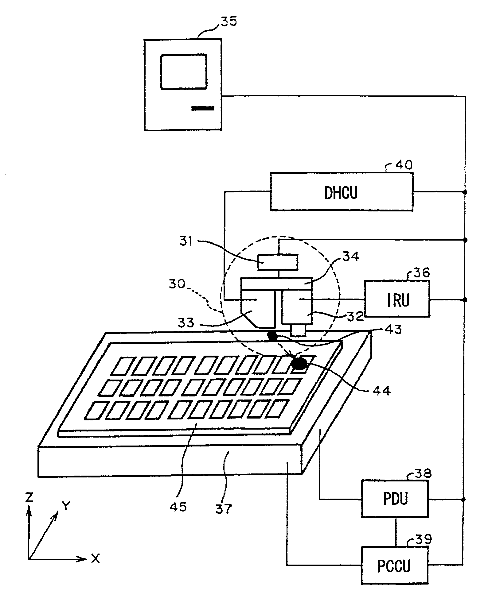
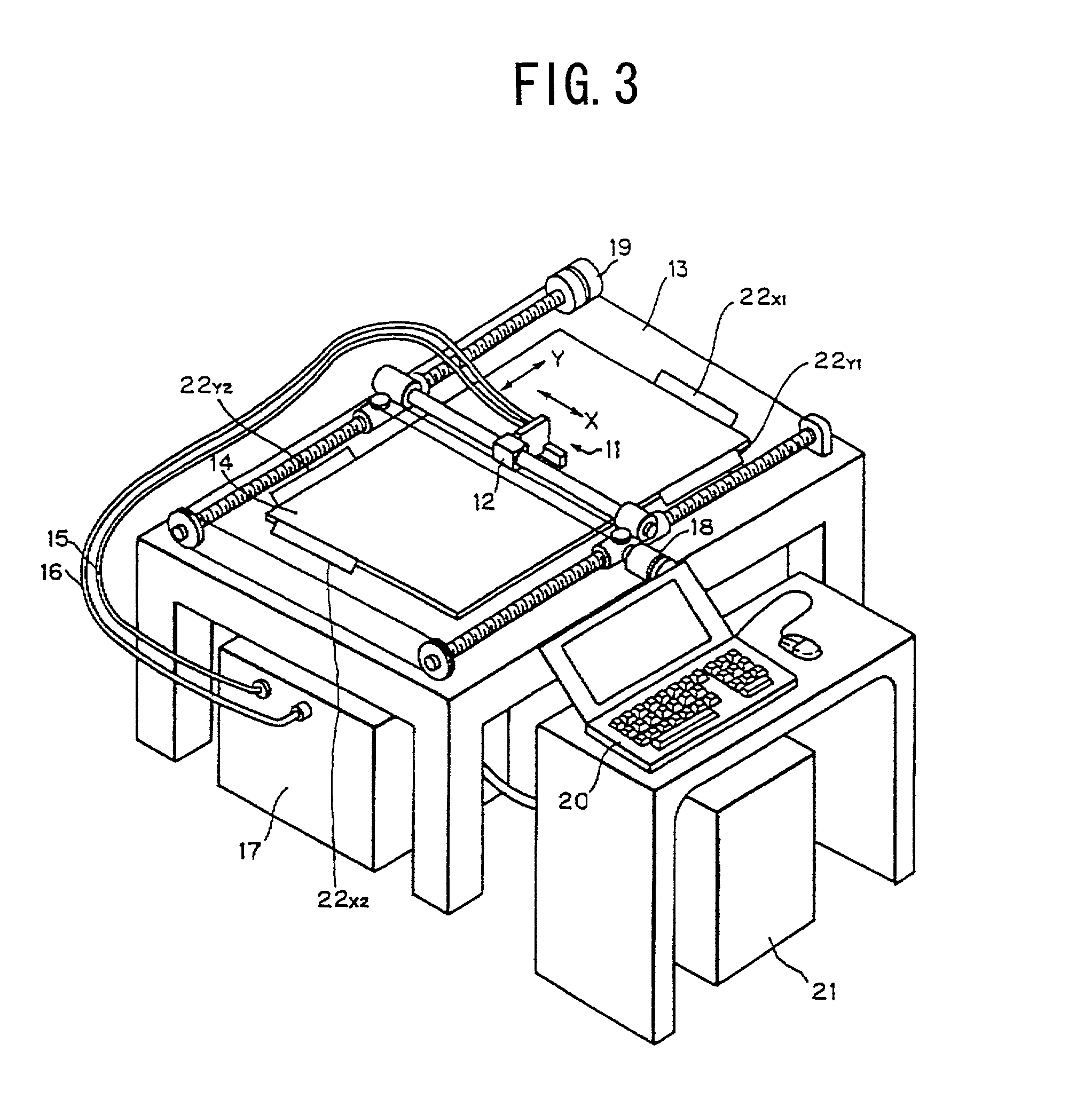
[0061]A description will now be provided of preferred embodiments of the present invention with reference to the accompanying drawings.

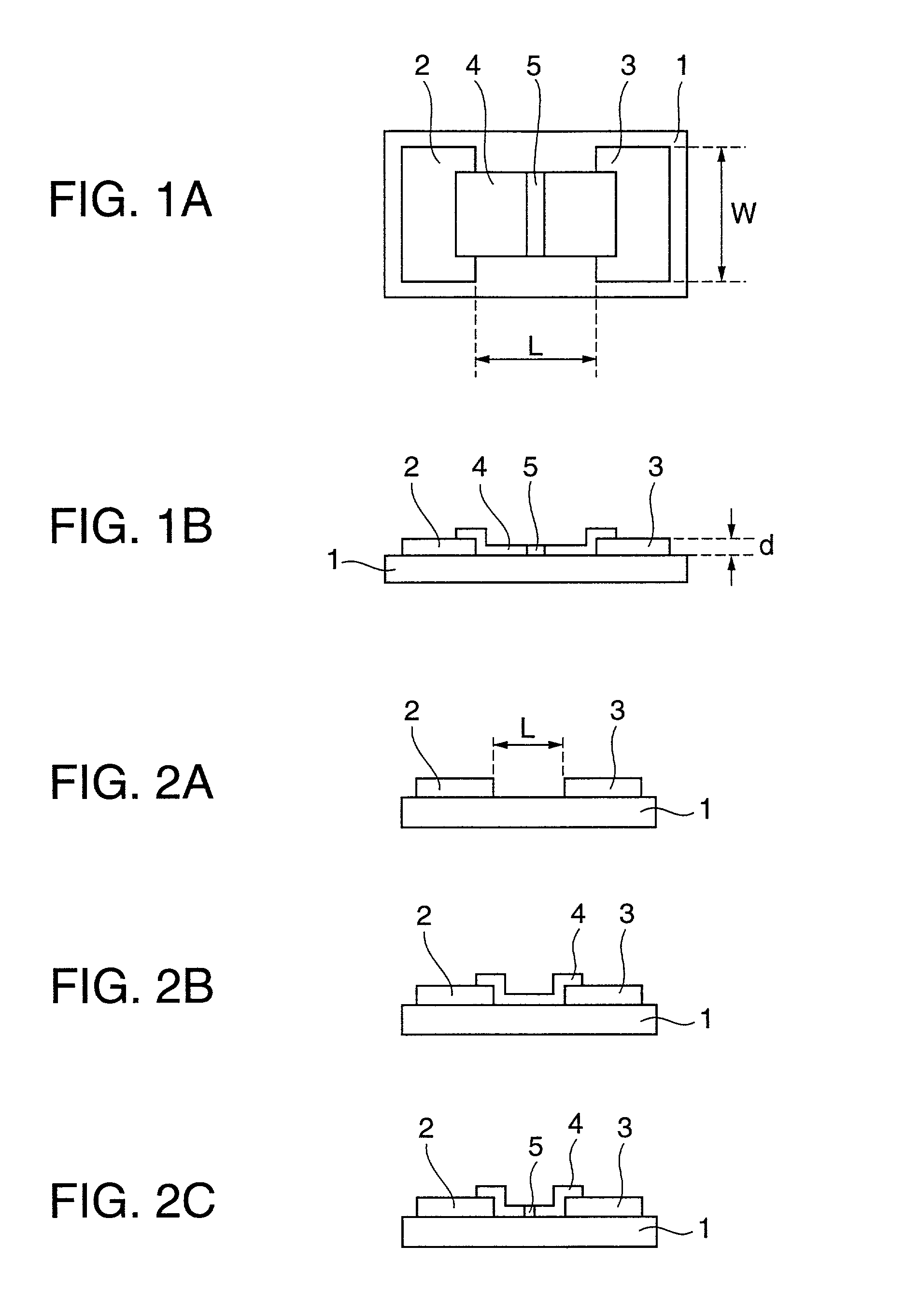
[0062]FIG. 1A and FIG. 1B shows one embodiment of the electron-emitting device which is produced by the production apparatus of the present invention. FIG. 1A is a plan view of the electron-emitting device, and FIG. 1B is a cross-sectional view of the electron-emitting device.

[0063]For the sake of simplicity of description, the electron-emitting device of the present embodiment is provided with a single surface conduction electron-emitting element as shown in FIG. 1A and FIG. 1B. However, in practical applications, a plurality of surface conduction electron-emitting elements are arrayed in a matrix formation in the electron-emitting device.

[0064]As shown in FIG. 1A and FIG. 1B, in the electron-emitting device of the present embodiment, a substrate 1, a pair of opposing electrodes 2 and 3, a conductive thin film 4, and an electron-emitting region 5 ar...


PUM


Abstract

An electron-emitting device and an image display apparatus in which the electron-emitting device is provided. In the electron-emitting device, a substrate has sides in two orthogonal first directions. A plurality of pairs of electrodes are disposed on the substrate. A conductive thin film is disposed between each of the electrode pairs. A plurality of surface conduction electron-emitting elements are disposed in the conductive thin film by discharging drops of a source material of the film thereto, each electron-emitting element spaced apart from the opposing electrodes of one of the electrode pairs. The electron-emitting elements are arrayed in a matrix formation, the matrix having rows and columns in two orthogonal second directions, the electron-emitting elements being disposed such that the second directions of the matrix are parallel to the first directions of the substrate.

Description

BACKGROUND OF THE INVENTION[0001]1. Field of the Invention[0002]The present invention relates to an electron-emitting device using surface conduction electron-emitting elements, and an image display apparatus in which the electron-emitting device is provided. Further, the present invention relates to an apparatus for production of the electron-emitting device.[0003]2. Description of the Related Art[0004]Conventional electron emission sources for emitting electrons are classified into two major types: hot-cathode devices and cold-cathode devices. The cold-cathode devices include FE (field emission) type, MIM (metal / insulator / metal) type, and surface conduction type. The FE type electron emission devices are, for example, disclosed in “Field Emission” Advance in Electron Physics, vol. 8, p.89, 1956, by W. P. Dyke & W. W. Dolan and “Physical Properties of Thin-Film Field Emission Cathodes with Molybdenum” J. Appl. Phys., 475248, 1976, by C. A. Spindt. The MIM type electron emission dev...

Claims


Application Information

Patent Timeline
Patent Type & Authority Patents(United States)
IPC IPC(8): H01J1/62B41J2/01B41J3/407H01J1/316H01J9/02H01J29/04H01J31/12
CPCB41J2/125B41J3/4073H01J1/316H01J31/127H01J9/027B41J2202/09Y10T428/24174H01J2201/3165H01J2329/0489Y10T428/24752
Inventor SEKIYA, TAKURO
Owner RICOH KK
Why Eureka
Try Eureka