
Eureka
For R&D, Eureka makes reading and utilizing patents & technical documents easy.
Eureka AIR
Designed for self-driven R&D workflows. Generate viable solutions, solve complex R&D challenges, empower your innovation with AI.

Eureka Materials
Designed for material experts only. Revolutionize your material R&D, from search, analyze, to developing new materials.

TechResearch
Generate reliable direction feasibility study reports for your R&D in just a few steps.

TechSeek
Discover and master advanced knowledge NOW. Basics, ideas, possibilities, all at once.

TechMind
As an expert in R&D Theories, TechMind can generates customized viable solutions instantly.

TechRisk
Analyze your overall solution with one click, know your potential R&D risks in advance.

TechMonitor
Get weekly tech updates, stay abreast of the latest tech innovations and key insights.
Electron-emitting device having a fissure to increase electron emission efficiency
- Summary
- Abstract
- Description
- Claims
- Application Information
AI Technical Summary
Benefits of technology
Problems solved by technology
Method used
Image

Examples
embodiments
[0085](Electron-Emitting Device)
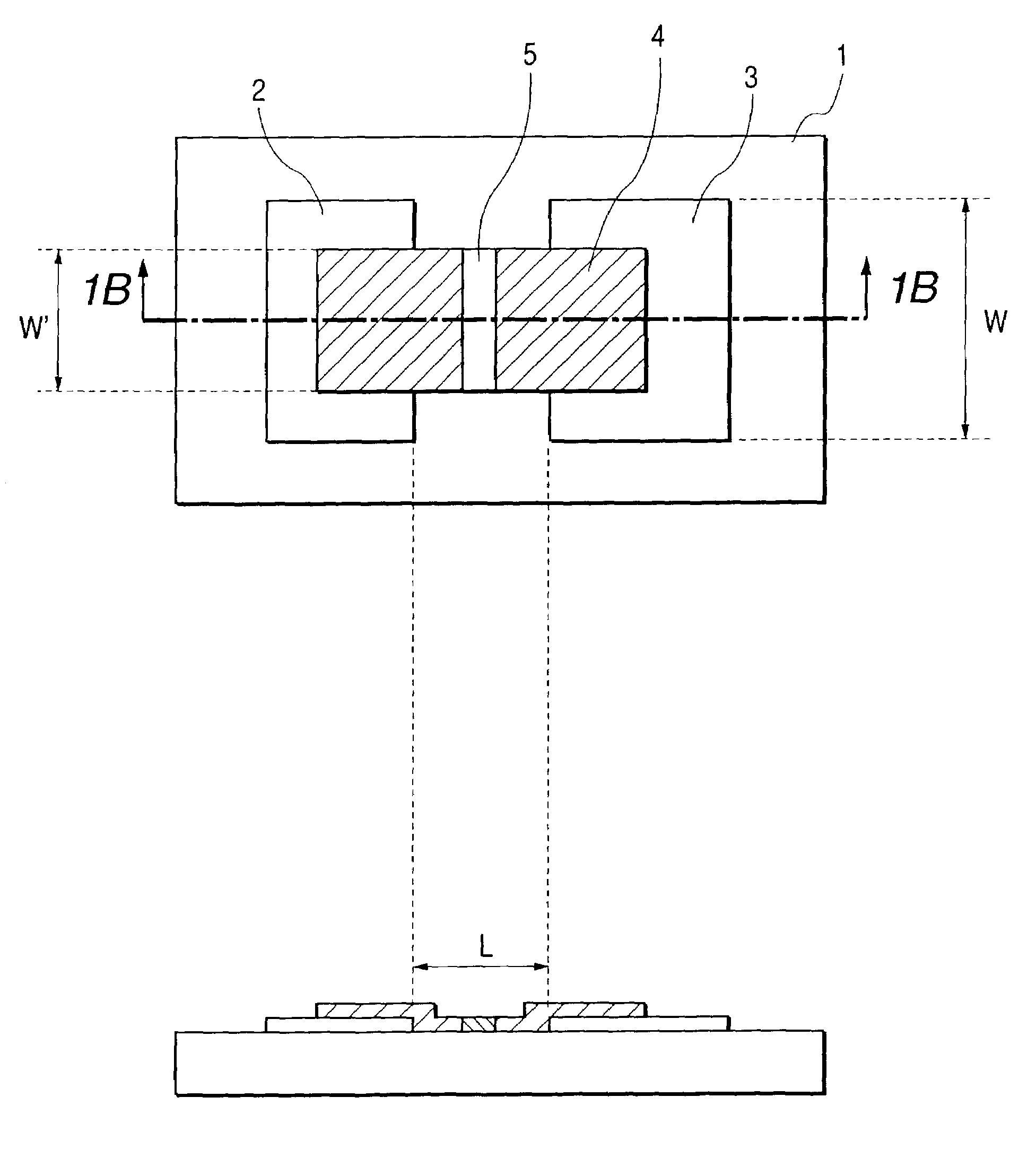
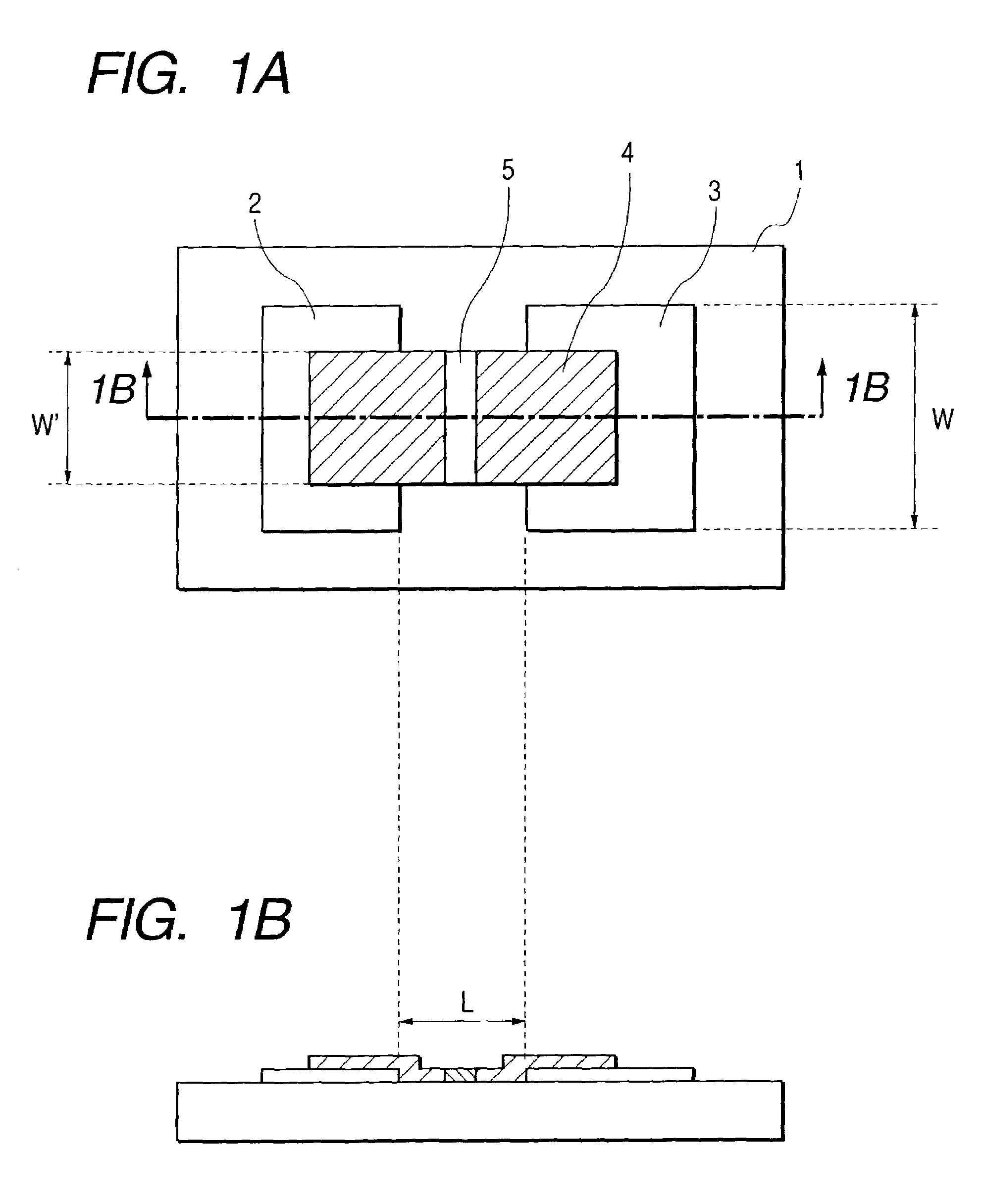
[0086]A specific embodiment of an electron-emitting device according to the present invention will be described with reference to the conceptual diagram of FIGS. 1A and 1B.
[0087]In FIGS. 1A and 1B, reference numeral 1 denotes a glass substrate corresponding to a substrate, reference numerals 2 and 3 denote device electrodes corresponding to electrodes, and reference numeral 4 denotes an electroconductive film having a fissure, which is connected with the device electrodes 2 and 3. Further, reference numeral 5 denotes an electron-emitting portion including the fissure formed in the electroconductive film 4. The present invention has a characteristic in this fissure.
[0088]That is, according to the present invention, it is characterized in that a fissure region of 95% or more of a length in the fissure direction has a fissure width of from 60 nm to 800 nm and a difference of 300 nm or less between a maximum value and a minimum value of the fissure width....
example 1
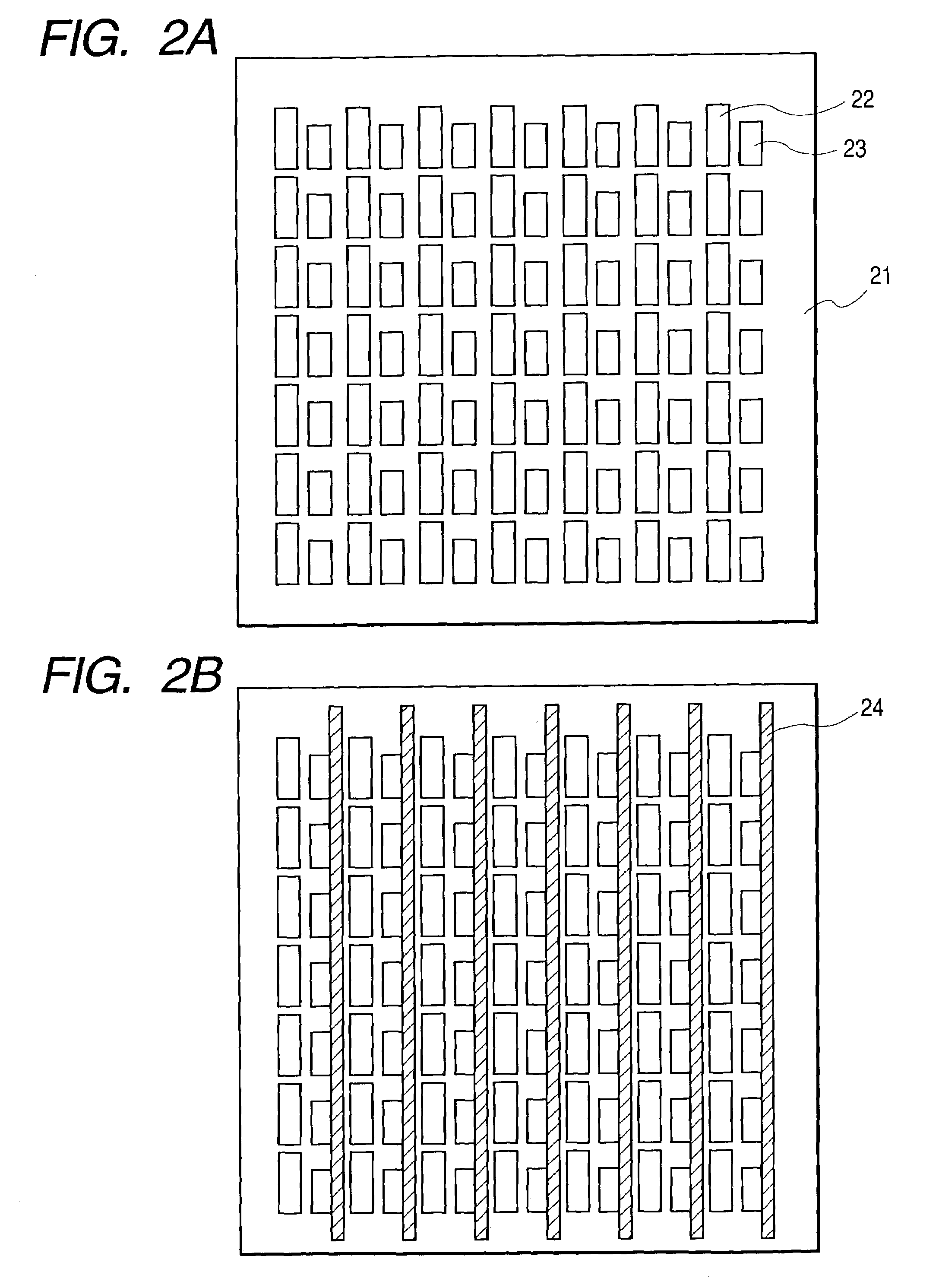
[0192](A) Formation of Device Electrode
[0193]This example employed glass of PD-200 (manufactured by ASAHI GLASS CO., LTD.) containing a little alkaline ingredient which has a thickness of 2.8 mm and a size of 350×300 (mm). Further, the glass was used after coating and baking thereon 100 nm of an SiO2 film as a sodium blocking layer.
[0194]In addition, device electrodes 22 and 23 were formed on a glass substrate 21 by the following process. That is, by sputtering, a film of titanium (Ti) having a thickness of 5 nm was first formed as a base layer and a film of platinum (Pt) having a thickness of 40 nm was formed thereon. Thereafter, a photo resist was applied and patterning was conducted by photolithography including a series of steps, exposure, development, and etching.
[0195]In this example, an interval L between the device electrodes was 10 μm and W thereof was 100 μm.
[0196](B) Formation of Y Directional Wiring
[0197]A Y directional wiring as a common wiring was formed with a linear ...
PUM
 Abstract
Description
Claims
Application Information
 - R&D Engineer
- R&D Manager
- IP Professional
- Industry Leading Data Capabilities
- Powerful AI technology
- Patent DNA Extraction
Browse by: Latest US Patents, China's latest patents, Technical Efficacy Thesaurus, Application Domain, Technology Topic, Popular Technical Reports.
© 2024 PatSnap. All rights reserved.Legal|Privacy policy|Modern Slavery Act Transparency Statement|Sitemap|About US| Contact US: help@patsnap.com