High-performance CMOS SOI devices on hybrid crystal-oriented substrates

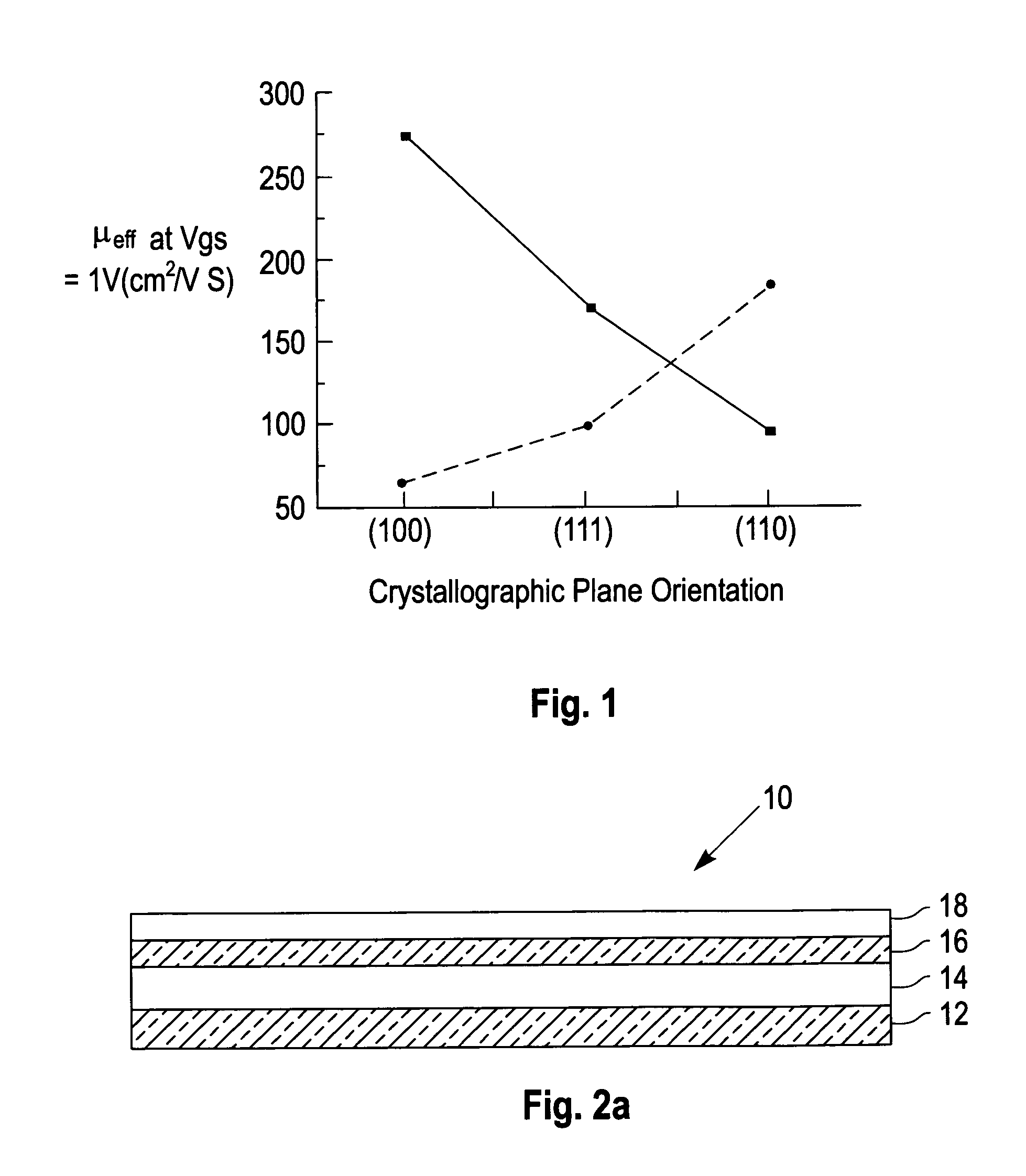
a technology of crystal-oriented substrates and cmos soi, which is applied in the direction of semiconductor devices, electrical apparatus, transistors, etc., can solve the problems of significant deformation of electron mobilities on (110) si surfaces, undesirable nfets having larger widths, and completely inappropriate crystal orientation for nfet devices

Inactive Publication Date: 2006-02-07
INT BUSINESS MASCH CORP
View PDF3 Cites 353 Cited by
  • Summary
  • Abstract
  • Description
  • Claims
  • Application Information

AI Technical Summary

Benefits of technology

[0013]Thus, the invention provides a structure that utilizes a type of crystal orientation that benefits N-type transistors for the substrate portions that are below the N-type transistors and a different type of crystal orientation for the substrate portions that are below the P-type transistors that is more beneficial for P-type transistors. This allows each type of transistor to be formed on a different type of substrate with a crystal orientation that benefits each different type of transistor. Further, the invention can selectively include a strain producing layer on either or both types of transistors to allow each of the different types of transistors to be subject to the type straining that is most beneficial to each type of transistor.

Problems solved by technology

NFETs having larger widths are undesirable since they take up a significant amount of chip area.
Unfortunately, electron mobilities on (110) Si surfaces are significantly degraded compared to (100) Si surfaces.
As can be deduced from the above discussion and FIG. 1, the (110) Si surface is optimal for PFET devices because of excellent hole mobility, yet such a crystal orientation is completely inappropriate for NFET devices.

Method used


Image

  • High-performance CMOS SOI devices on hybrid crystal-oriented substrates
  • High-performance CMOS SOI devices on hybrid crystal-oriented substrates
  • High-performance CMOS SOI devices on hybrid crystal-oriented substrates

Examples


Embodiment Construction

[0021]The present invention and the various features and advantageous details thereof are explained more fully with reference to the nonlimiting embodiments that are illustrated in the accompanying drawings and detailed in the following description. It should be noted that the features illustrated in the drawings are not necessarily drawn to scale. Descriptions of well-known components and processing techniques are omitted so as to not unnecessarily obscure the present invention. The examples used herein are intended merely to facilitate an understanding of ways in which the invention may be practiced and to further enable those of skill in the art to practice the invention. Accordingly, the examples should not be construed as limiting the scope of the invention.

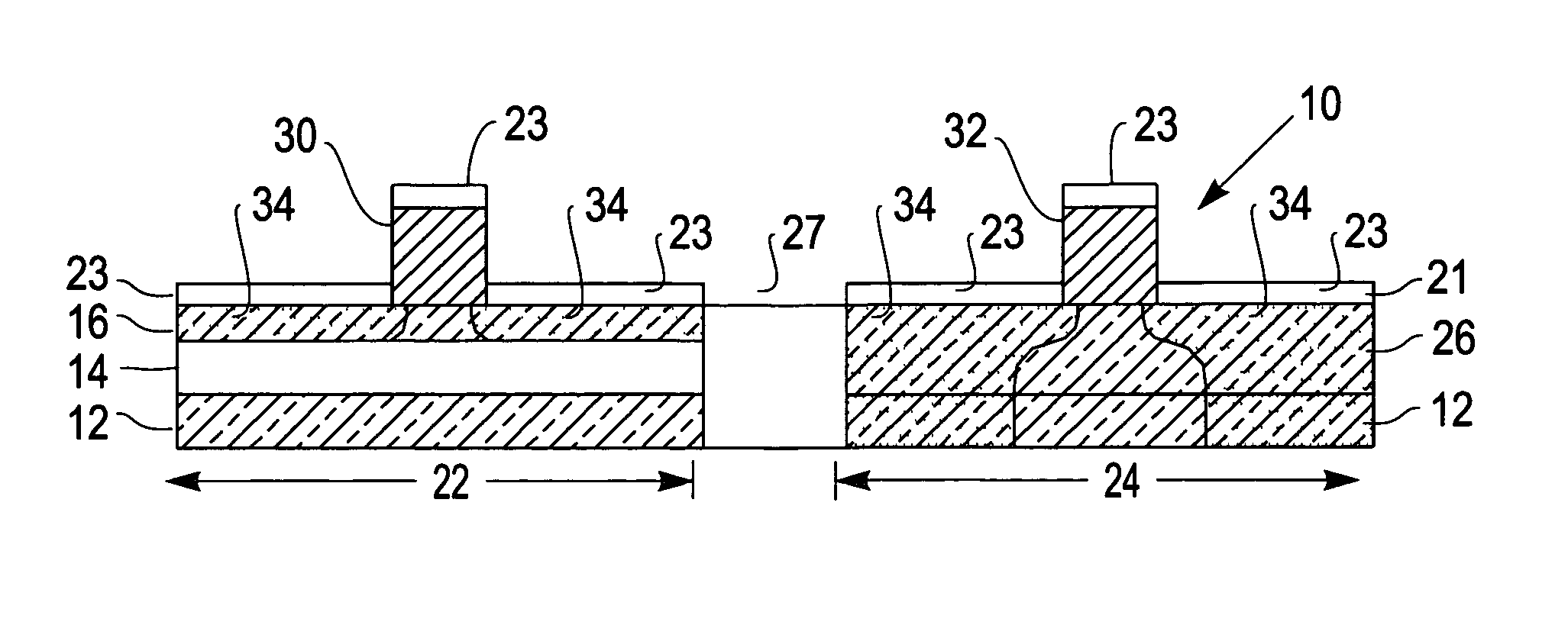
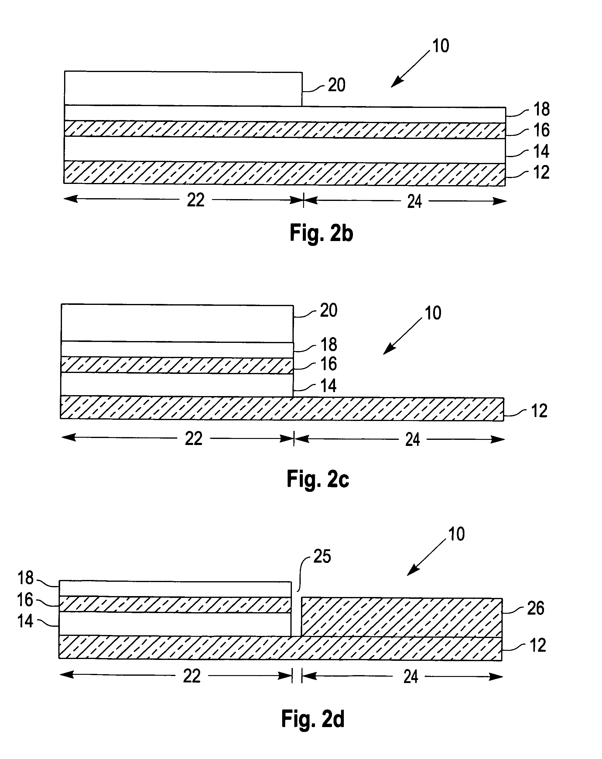
[0022]The present invention, which provides a method of forming different semiconductor devices, such as NFETs and PFETS, onto a bonded substrate having different crystallographic surfaces, with strained channel regions, wil...


PUM


Abstract

Disclosed is an integrated circuit structure that has a substrate having at least two types of crystalline orientations. The first-type transistors are on first portions of the substrate that have a first type of crystalline orientation and second-type transistors are on second portions of the substrate that have a second type of crystalline orientation. The straining layer is above the first-type transistors and the second-type transistors. Further, the straining layer can be strained above the first-type transistors and relaxed above the second-type transistors.

Description

BACKGROUND OF INVENTION[0001]1. Field of the Invention[0002]The present invention relates to semiconductor devices, and more particularly to integrated semiconductor devices, such as silicon-on-insulator (SOI) / complementary metal oxide semiconductor (CMOS) devices, that are formed on a hybrid crystal oriented substrate. In particular, the present invention provides a means for integrating at least two types of semiconductor devices, such as NFETs and PFETs, onto a bonded substrate having different crystallographic orientations. The location of each device on the bonded substrate is dependent upon the performance of that device has on a particular crystal orientation. For example, the present invention forms NFETs on a (100) surface, while the PFETs are formed on a (110) surface. The (100) crystal surface provides NFETs with high performance, while the (110) crystal surface provides PFETs with high performance.[0003]2. Background of the Invention[0004]In present semiconductor technol...

Claims


Application Information

Patent Timeline
Patent Type & Authority Patents(United States)
IPC IPC(8): H01L29/04H01L27/01H01L29/00H01L31/036H01L21/762H01L21/02H01L21/76H01L21/82H01L21/8238H01L27/02H01L27/08H01L27/092H01L27/12H01L29/786
CPCH01L27/1203H01L27/1207H01L29/785
Inventor NOWAK, EDWARD J.
Owner INT BUSINESS MASCH CORP
Why Eureka
Try Eureka