Memory devices with page buffer having dual registers and method of using the same

a memory device and register technology, applied in electronic circuit testing, digital storage, instruments, etc., can solve the problems of a long time for data to load to a page of as many as 2048 bytes, a procedure, and a limitation,

Inactive Publication Date: 2006-02-07
SAMSUNG ELECTRONICS CO LTD
View PDF22 Cites 60 Cited by
  • Summary
  • Abstract
  • Description
  • Claims
  • Application Information

AI Technical Summary

Benefits of technology

[0159]One object of this invention is to solve this problem.

Problems solved by technology

Since the flash memory device stores information using tunneling via an insulation film, it takes some time to store information.
This procedure, however, has a limitation.
So, it takes a long time for data to load to a page of as many as 2048 bytes.
Another problem in the prior art is the copy back problem.
The prior art is limited as to how large the memory devices can become.
Accordingly, the information-storing characteristic of the NAND-type flash memory is seriously affected by the loading time.

Method used


Image

  • Memory devices with page buffer having dual registers and method of using the same
  • Memory devices with page buffer having dual registers and method of using the same
  • Memory devices with page buffer having dual registers and method of using the same

Examples


Embodiment Construction

[0052]As has been mentioned, the present invention provides semiconductor memory devices, and methods of using the same. The invention is now described in more detail.

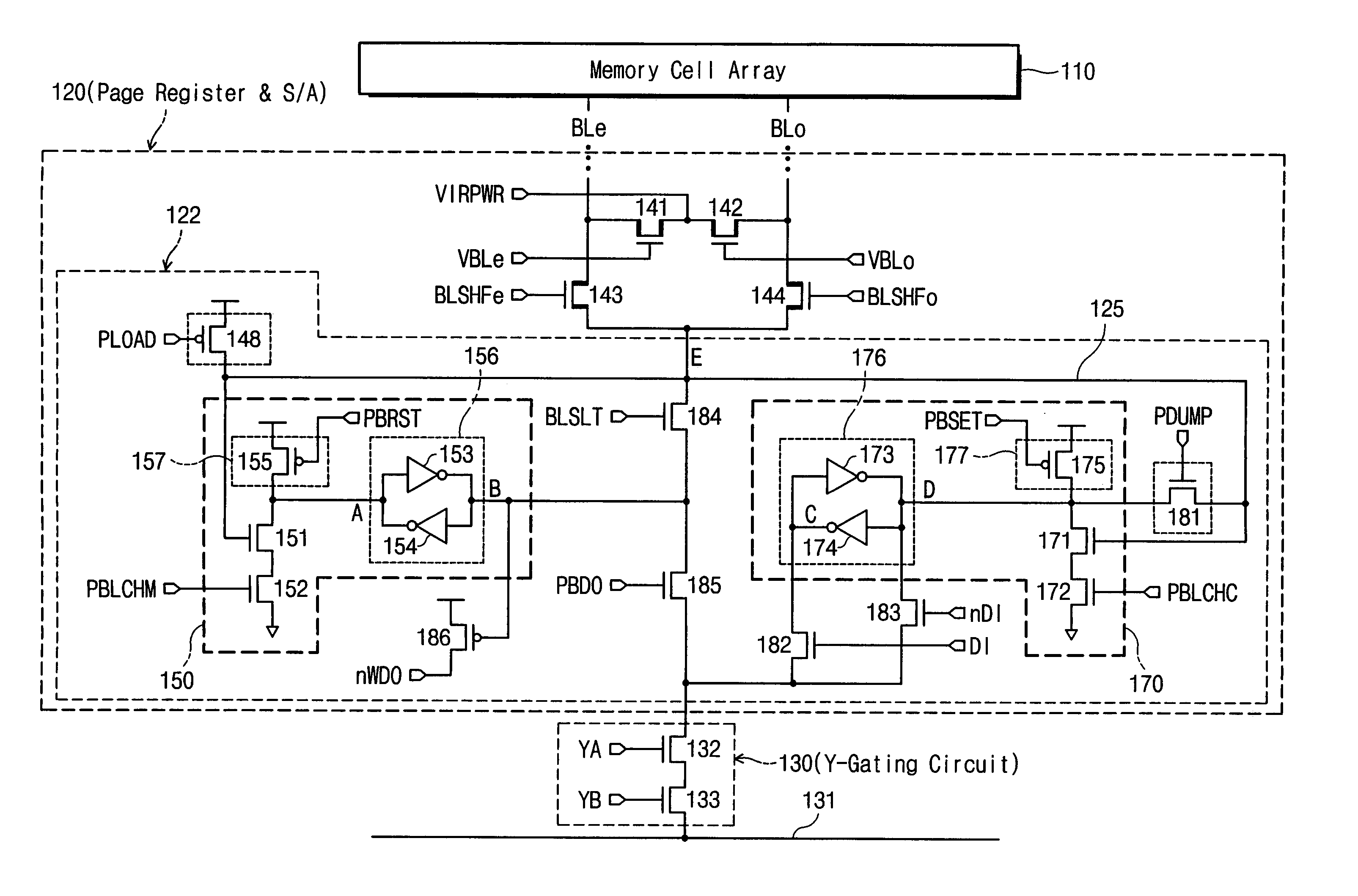
[0053]Referring now to FIG. 3, a memory device 100 made according to the invention is described. Memory device 100 may be a NAND flash memory. Memory device 100 has an array 110 of memory cells to store data, a Page Register and Sense Amplifier (S / A) block 120, and a Y-gating circuit 130 to gate data stored in a group of the memory cells. Page Register and S / A block 120 is coupled between memory cell array 110 and Y-gating circuit 130.

[0054]Page Register and S / A block 120 includes a page buffer 122. Page buffer 122 includes dual registers according to the invention, as will be described in more detail below.

[0055]Device 100 also includes additional components, such as X-buffers latches and decoders, Y-buffers latches and decoders, a command register, a Control Logic and High Voltage Generator, and global buffers. They ...


PUM


Abstract

A nonvolatile memory device and programming method and apparatus therefore are described that include operatively coupled first and second sense amplifiers having first and second data registers or latches, a storage circuit for storing a data of the second amplifier, a pass / fail check circuit for checking the content of the second data register whether a cell of the memory device has been sufficiently programmed and a restore circuit for resetting the second data register for reprogramming the device until sufficiently programmed.

Description

[0001]This application is a continuation of U.S. patent application Ser. No. 10 / 315,897, filed Dec. 9, 2002, which is a continuation-in-part of U.S. patent application Ser. No. 10 / 013,191, filed Dec. 7, 2001, now issued U.S. Pat. No. 6,671,204 which claims priority from U.S. Provisional Application No. 60 / 307,572 filed on Jul. 23, 2001, all of which are hereby incorporated by reference in their entirety.BACKGROUND OF THE INVENTION[0002]1. Field of the Invention[0003]The present invention is related to the field of semiconductor memory devices and, more specifically, to a flash memory device with a page buffer circuit having dual registers.[0004]2. Description of the Related Art[0005]The recent trends in semiconductor memory devices are for high integration, large capacity, and to support systems operating at high speeds. These trends are for both volatile memories (e.g., DRAM and SRAM) and non-volatile memories (e.g., flash memories).[0006]Flash memories are generally subdivided int...

Claims


Application Information

Patent Timeline
Patent Type & Authority Patents(United States)
IPC IPC(8): G11C7/00G01R31/28G11C7/10G11C11/34G11C16/02G11C16/04G11C16/06G11C16/10G11C16/24G11C16/34G11C29/12
CPCG11C7/1006G11C7/1039G11C7/1051G11C7/106G11C7/1069G11C7/1078G11C7/1087G11C7/1093G11C16/0483G11C16/10G11C16/12G11C16/24G11C16/26G11C16/3454G11C16/3459G11C7/1021G11C2216/14G11C2207/002G11C16/04G01R31/28
Inventor LEE, JUNEKWON, OH-SUKIM, HEUNG-SOO
Owner SAMSUNG ELECTRONICS CO LTD
Why Eureka
Try Eureka