Laser beam processing machine

a laser beam and processing machine technology, applied in the direction of soldering apparatus, manufacturing tools,auxillary welding devices, etc., can solve the problems of chip or crack production on the cut surface of semiconductor chips, reduced productivity, and limited feed ra

Active Publication Date: 2006-02-14
DISCO CORP
View PDF6 Cites 136 Cited by
  • Summary
  • Abstract
  • Description
  • Claims
  • Application Information

AI Technical Summary

Benefits of technology

[0009]To attain the above object, according to the present invention, there is provided a laser beam processing machine comprising a chuck table for holding a workpiece and a laser beam application means for applying a laser beam to the workpiece held on the chuck table, wherein the machine further comprises a protective film forming means for forming a protective film on a surface to be processed of the workpiece before the laser beam processing.
[0010]The above protective film forming means comprises a spinner table that holds the workpiece and rotates and a resin solution supply means for supplying a liquid resin solution to the to-be-processed surface of the workpiece held on the spinner table. Preferably, the liquid resin solution supplied by the above resin solution supply means is water-soluble. Preferably, the above protective film forming means comprises a cleaning water supply means for supplying cleaning water to the to-be-processed surface of the workpiece held on the spinner table.

Problems solved by technology

When the semiconductor wafer is cut with such a cutting blade, chips or cracks are produced on the cut surface of the semiconductor chip.
If the size of the semiconductor chip is reduced, however, the proportion of the streets to the semiconductor chip increases to cause reduction in productivity.
In cutting with the cutting blade, further, problems are posed that the feed rate is limited and the semiconductor chips are contaminated with chips produced by cutting.
When the semiconductor wafer having the low dielectric constant insulating film (Low-k film) laminated thereon is cut with a cutting blade along the streets, there arises a problem that the Low-k film peels off.
Or when the semiconductor wafer having a metal pattern called the test element group “Teg” applied thereto is cut with a cutting blade along streets, another problem arises that burrs are produced because the metal pattern is made of a tacky metal such as copper or the like.
Although since the method of cutting by applying a laser beam is to cut a semiconductor wafer along streets with a laser beam, it can solve the above problems that the Low-k film peels off and that burrs are produced, this method creates a new problem that when a laser beam is applied along the streets of the semiconductor wafer, thermal energy is concentrated on the exposed areas to produce debris which adhere to bonding pads that are connected to a circuit and the like, thereby reducing the quality of the semiconductor chip.
However, that a protective film forming apparatus for forming a protective film on the to-be-processed surface of a workpiece and a laser beam processing machine for applying a laser beam to the workpiece through the protective film are independently installed is not always efficient from the viewpoints of a factory space and the conveyance of a workpiece between apparatuses.

Method used


Image

  • Laser beam processing machine
  • Laser beam processing machine
  • Laser beam processing machine

Examples


Embodiment Construction

[0022]Preferred embodiments of a laser beam processing machine constituted according to the present invention will be described in detail hereinbelow with reference to the accompanying drawings.

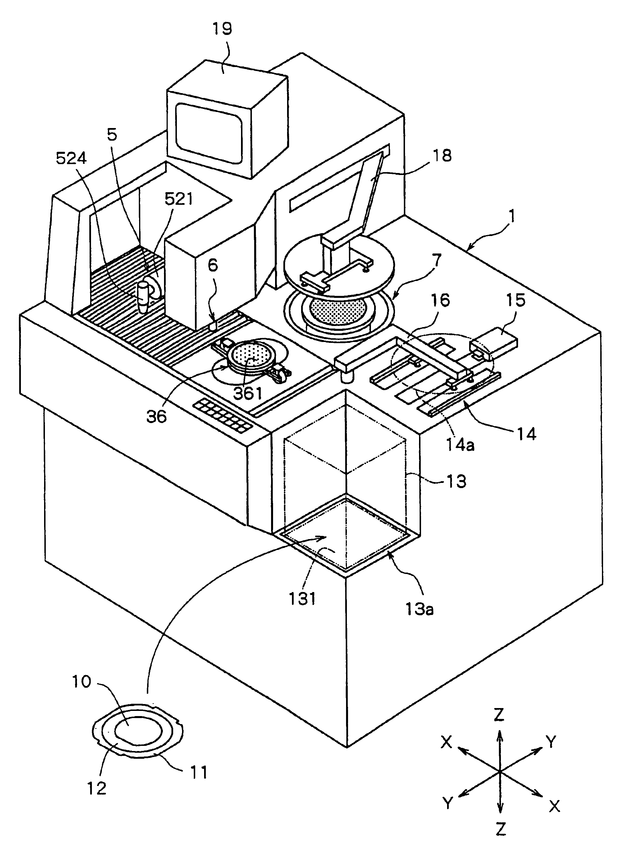
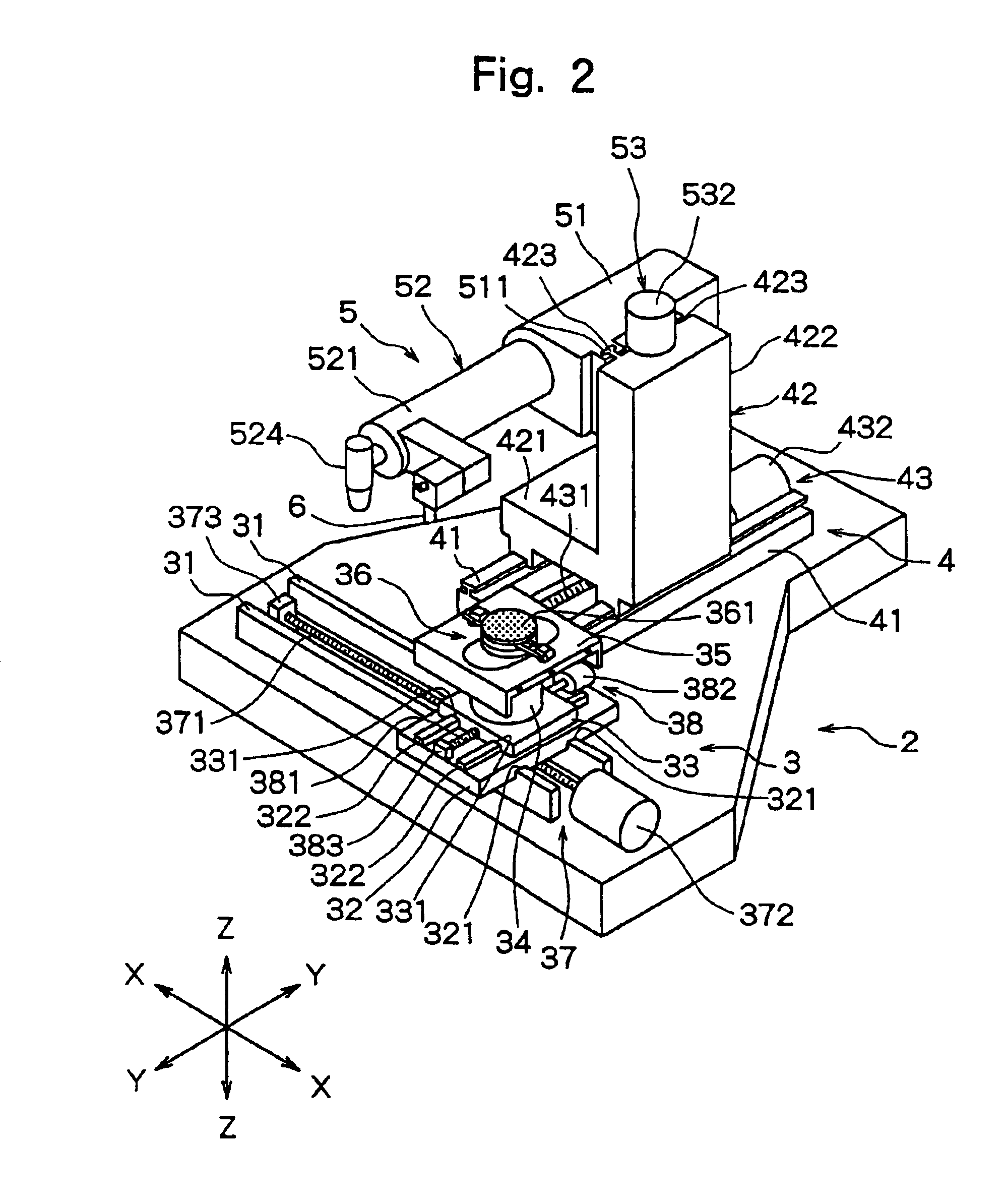
[0023]FIG. 1 is a perspective view of the laser beam processing machine constituted according to the present invention. The laser beam processing machine shown in FIG. 1 comprises a substantially rectangular parallelepiped housing 1. In this housing 1, there are installed a stationary base 2 shown in FIG. 2, a chuck table unit 3 for holding a workpiece, which is mounted on the stationary base 2 in such a manner that it can move in a direction indicated by an arrow X, a laser beam application unit support mechanism 4 arranged on the stationary base 2 in such a manner that it can move in a direction indicated by an arrow Y perpendicular to the direction indicated by the arrow X, and a laser beam application unit 5 arranged on the laser beam application unit support mechanism 4 in such a manner ...


PUM

PropertyMeasurementUnit
particle diameteraaaaaaaaaa
widthaaaaaaaaaa

Abstract

A laser beam processing machine comprising a chuck table for holding a workpiece and a laser beam application means for applying a laser beam to the workpiece held on the chuck table, wherein the machine further comprises a protective film forming means for forming a protective film on the to-be-processed surface of the workpiece before laser beam processing.

Description

FIELD OF THE INVENTION[0001]The present invention relates to a laser beam processing machine for carrying out a predetermined processing by applying a laser beam to a predetermined area of a workpiece.DESCRIPTION OF THE PRIOR ART[0002]As known to people of ordinary skill in the art, in the semiconductor device manufacturing process, individual semiconductor chips are manufactured by cutting a substantially disk-like semiconductor wafer having a plurality of areas sectioned by streets (cutting lines) arranged in a lattice pattern on its surface, and a circuit such as IC, LSI or the like formed in each of the sectioned areas, along the streets. Cutting along the streets of the semiconductor wafer is generally carried out by a cutting machine called “a dicer”. This cutting machine comprises a chuck table for holding the semiconductor wafer as a workpiece, a cutting means for cutting the semiconductor wafer held on the chuck table, and a moving means for moving the chuck table and the c...

Claims


Application Information

Patent Timeline
Patent Type & Authority Patents(United States)
IPC IPC(8): B23K26/00B23K26/10B23K26/18B23K26/40B23K37/047B23K101/40B28D1/22B28D5/00H01L21/301H01L21/78
CPCB23K26/0853B23K26/0884B23K26/18B23K26/4075H01L21/78B23K37/047B28D1/221B28D5/0058B23K26/422B23K2201/40B23K26/40B23K26/702B23K2101/40B23K2103/50
Inventor SEKIYA, KAZUMAYOSHIKAWA, TOSHIYUKI
Owner DISCO CORP
Why Eureka
Try Eureka