Solid-state logarithmic image sensing device

a logarithmic image and sensing device technology, applied in the field of solid-state logarithmic image sensing devices, can solve the problems of narrow dynamic range, flat blackness in dim portions of obtained images, and saturation in bright portions, and achieve the effect of high resolution and quick respons

Inactive Publication Date: 2006-02-14
SONY SEMICON SOLUTIONS CORP
View PDF3 Cites 14 Cited by
  • Summary
  • Abstract
  • Description
  • Claims
  • Application Information

AI Technical Summary

Benefits of technology

[0011]An object of the present invention is to provide an image-sensing apparatus that permits shooting of a subject having a wide brightness range, ranging from a high-brightness region to a low-brightness region, with high resolution and that permits individual pixels to be reset to their original state quickly even in a low-brightness region and thereby offers quick response.

Problems solved by technology

A CCD-type image-sensing device accumulates photoelectric charges in potential wells while transferring them, and has the disadvantage of a comparatively narrow dynamic range.
This, however, leads to a narrow dynamic range and thus demands accurate control of the amount of exposure.
Moreover, even if the amount of exposure is controlled accurately, the obtained image tends to suffer from flat blackness in dim portions thereof and saturation in bright portions thereof.
However, in a low-brightness region, under the influence of the threshold voltage of the MOS transistor, the reset current has difficulty in flowing into the MOS transistor.
Therefore, it is difficult for the photoelectric charge accumulated in the MOS transistor to recombine with the reset current, and thus resetting takes an unduly long time.
In this way, in a low-brightness region, the individual pixels exhibit poor response, and this causes an after-image to appear in immediately subsequent image sensing.

Method used


Image

  • Solid-state logarithmic image sensing device
  • Solid-state logarithmic image sensing device
  • Solid-state logarithmic image sensing device

Examples


first embodiment

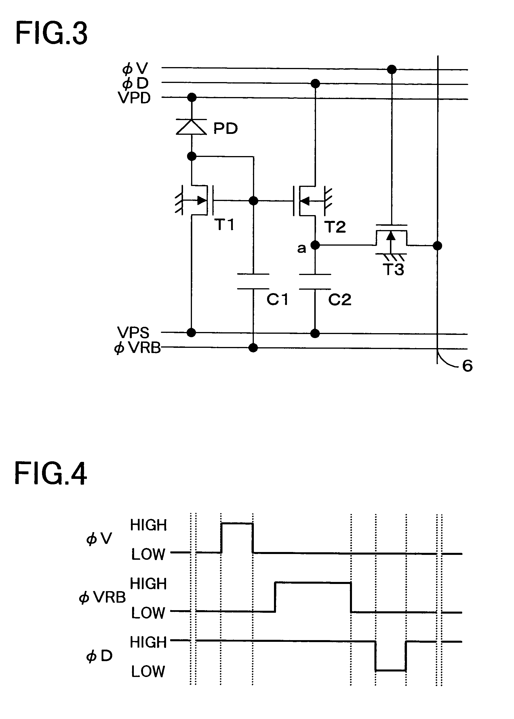
[0057]Now, a first embodiment (FIG. 3) of the invention, which is applicable to each pixel of the first example of the pixel configuration shown in FIG. 2, will be described with reference to the drawings.

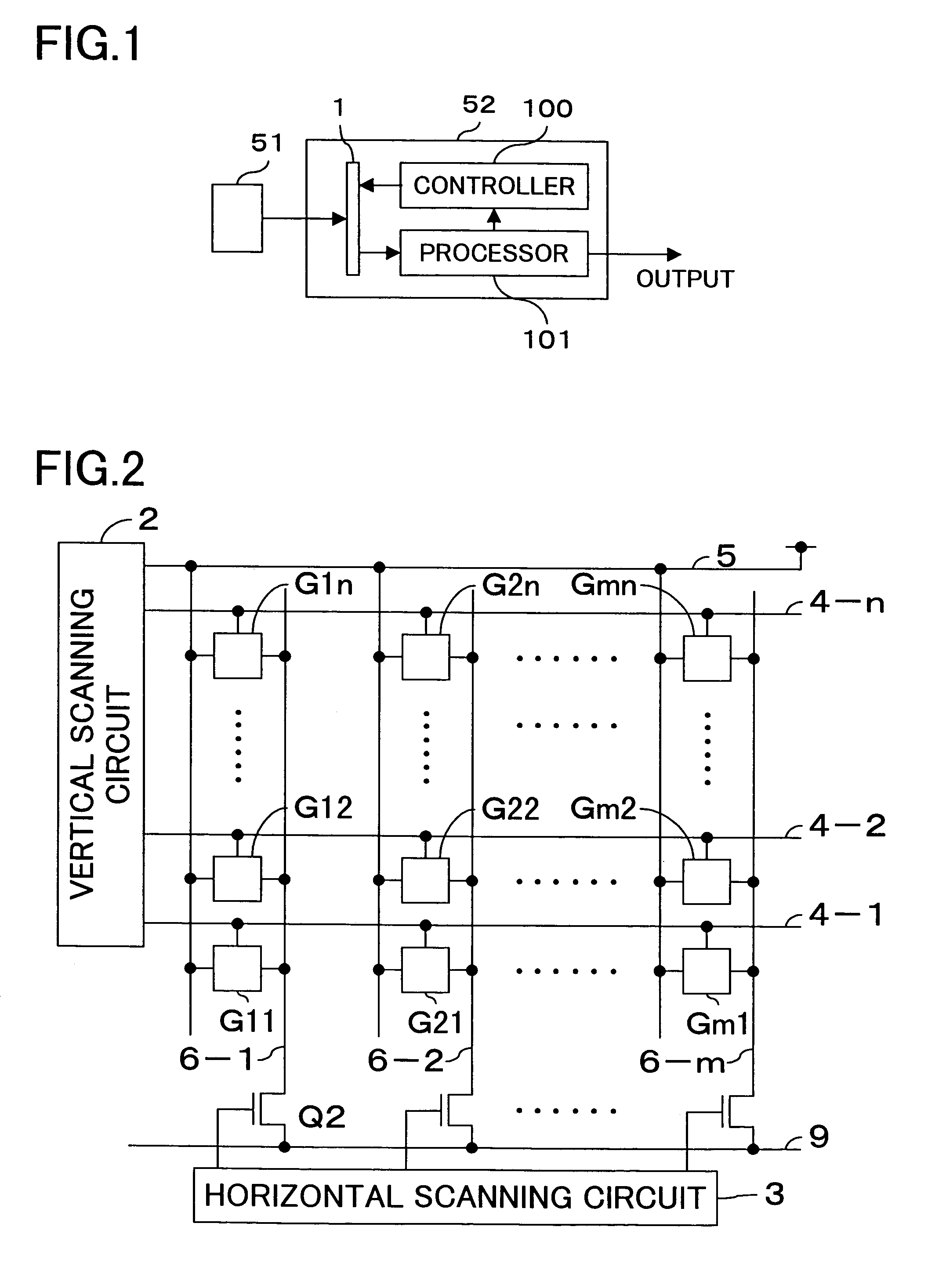
[0058]In FIG. 3, a pn photodiode PD serves as a photosensitive element (photoelectric conversion portion). The anode of this photodiode PD is connected to the gate and drain of a first MOS transistor T1, and also to the gate of a second MOS transistor T2. The source of the MOS transistor T2 is connected to the drain of a third MOS transistor T3 for selecting a row. The source of this MOS transistor T3 is connected to the output signal line 6 (this output signal line 6 corresponds to the output signal lines 6-1, 6-2, . . . , 6-m in FIG. 2). The MOS transistors T1 to T3 are all N-channel MOS transistors, and have their back gates grounded.

[0059]A direct-current voltage VPD is applied to the cathode of the photodiode PD. On the other hand, a direct-current voltage VPS is applied to th...

second embodiment

[0070]Next, a second embodiment of the invention will be described with reference to the drawings. FIG. 6 is a circuit diagram showing the configuration of each pixel of the solid-state image-sensing device of this embodiment. It is to be noted that such elements, signal lines, and others as are used for the same purposes here as in the pixel shown in FIG. 3 are identified with the same reference symbols, and their detailed descriptions will be omitted.

[0071]As shown in FIG. 6, in this embodiment, a signal φVPS is fed to the source of the MOS transistor T1, and the capacitor C1 is omitted. In other respects, each pixel of this embodiment is configured in the same manner as in the first embodiment (FIG. 3). The signal φVPS is a binary signal that takes one of two predetermined levels, i.e. either a low level or a high level, at a time. Here, a high level refers to a voltage that is approximately equal to the direct-current voltage VPS and that causes the MOS transistor T1 to operate ...

third embodiment

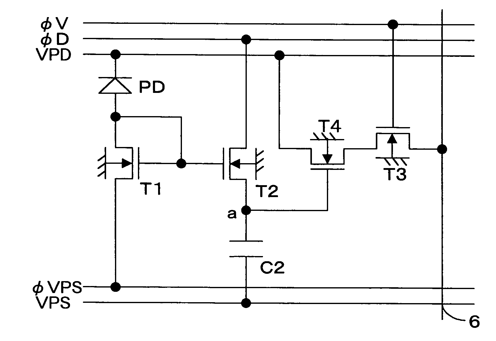
[0086]Next, a third embodiment of the invention, which is applicable to each pixel of the second example of the pixel configuration shown in FIG. 9, will be described with reference to the drawings. FIG. 11 is a circuit diagram showing the configuration of each pixel of the solid-state image-sensing device of this embodiment. It is to be noted that such elements, signal lines, and others as are used for the same purposes here as in the pixel shown in FIG. 3 are identified with the same reference symbols, and their detailed descriptions will be omitted.

[0087]As shown in FIG. 11, in this embodiment, as compared with the pixel shown in FIG. 3, there are provided additionally a fourth MOS transistor T4 having its gate connected to the node “a” for performing current amplification in accordance with the voltage at the node “a”, and a fifth MOS transistor T5 for initializing the potential at the node “a”. The source of the MOS transistor T3 is connected to the output signal line 6 (this o...


PUM


Abstract

In a solid-state image-sensing device, after completion of image sensing by individual pixels, in each pixel, a signal φVRB fed to a capacitor C1 connected to the gate of a first MOS transistor T1 is turned to a high level to make it easy for a negative electric charge to flow into the MOS transistor T1. This permits quick recombination of the positive electric charges accumulated at the drain and gate of the MOS transistor T1, at the gate of a MOS transistor T2, at the anode of a photodiode, and in a capacitor C2, and thereby makes quick resetting possible.

Description

[0001]This application is based on applications Nos. H11-207696 and H11-208267 both filed in Japan on Jul. 22, 1999, the entire contents of which are hereby incorporated by reference.BACKGROUND OF THE INVENTION[0002]1. Field of the Invention[0003]The present invention relates to an image-sensing apparatus, and particularly to an image-sensing apparatus incorporating a solid-state image-sensing device having a plurality of pixels arranged therein.[0004]2. Description of the Prior Art[0005]Solid-state image-sensing devices designed for use in image-sensing apparatuses are not only small-sized, light-weight, and power-saving, but also free from image distortion, free from image burn-in, and resistant to unfavorable environmental conditions such as vibration and electric fields. Moreover, such image-sensing devices can be manufactured by a process common or analogous to one used to manufacture LSIs (large-scale integrated circuits), and therefore they are reliable and fit for mass produ...

Claims


Application Information

Patent Timeline
Patent Type & Authority Patents(United States)
IPC IPC(8): H04N5/335H04N5/225H04N5/235H04N5/355
CPCH04N3/155H04N5/35509H04N5/35518H04N5/235H04N23/70H04N25/571H04N25/573
Inventor HAGIHARA, YOSHIOTAKADA, KENJI
Owner SONY SEMICON SOLUTIONS CORP
Why Eureka
Try Eureka