Heatsinking electronic devices

a technology for electronic devices and heatsinks, which is applied in the direction of lighting and heating apparatus, semiconductor/solid-state device details, printed circuit non-printed electric components association, etc. it can solve the problems of increasing the manufacturing cost of the assembly of fig. 2a, forming metal insert regions b>28/b>, and poor thermal conductivity of the insulating core of the pwb

Inactive Publication Date: 2006-02-14
HONEYWELL INT INC
View PDF12 Cites 269 Cited by
  • Summary
  • Abstract
  • Description
  • Claims
  • Application Information

AI Technical Summary

Benefits of technology

[0018]A further advantage of the present invention is that devices 10 are easily replaceable. In some prior art arrangements, in order to obtain adequate thermal conduction to the heatsink it has been common to attach devices 10 to the PWB and / or the PWB to the heatsink using thermally conductive glue. The glue makes disassembly difficult or impossible. With the present, arrangement such glue is not needed and the array may be easily disassembled to unsolder and replace any or all of devices 10. This is a significant advantage.

Problems solved by technology

The insulating core of the PWB is generally a poor thermal conductor.
An adhesive provides the best heat conduction but prevents or greatly hinders replacement of defective LEDs and adds to the manufacturing cost of the assembly of FIG. 2A.
A further disadvantage of the arrangement of FIG. 2A is that forming metal insert regions 28 is costly.
This can be very costly since, in general, standard heatsinks cannot be used and must be custom machined for each PWB configuration.
This is a significant disadvantage, especially where the PWB contains a large number of high power dissipation devices.

Method used


Image

  • Heatsinking electronic devices
  • Heatsinking electronic devices
  • Heatsinking electronic devices

Examples


Embodiment Construction

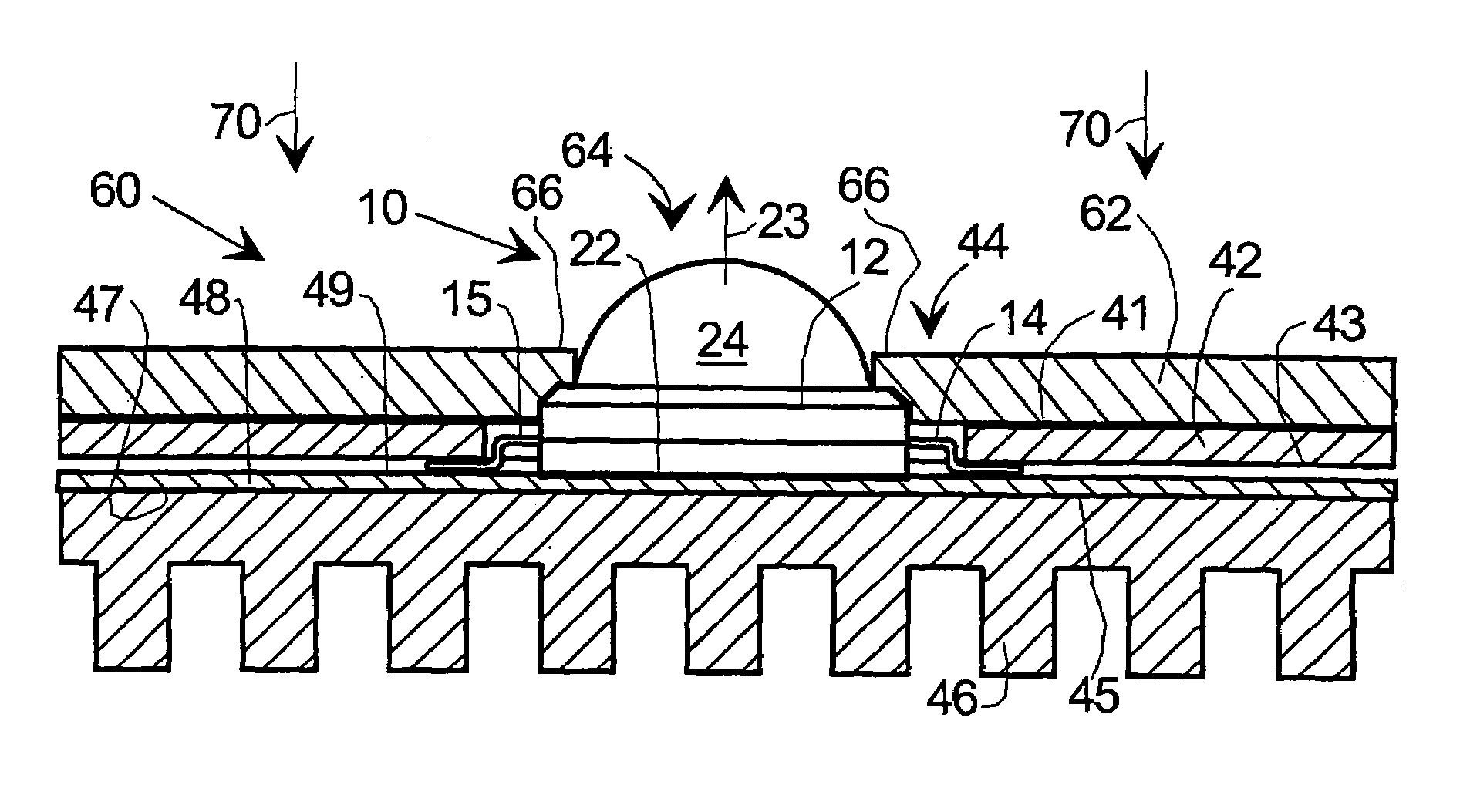
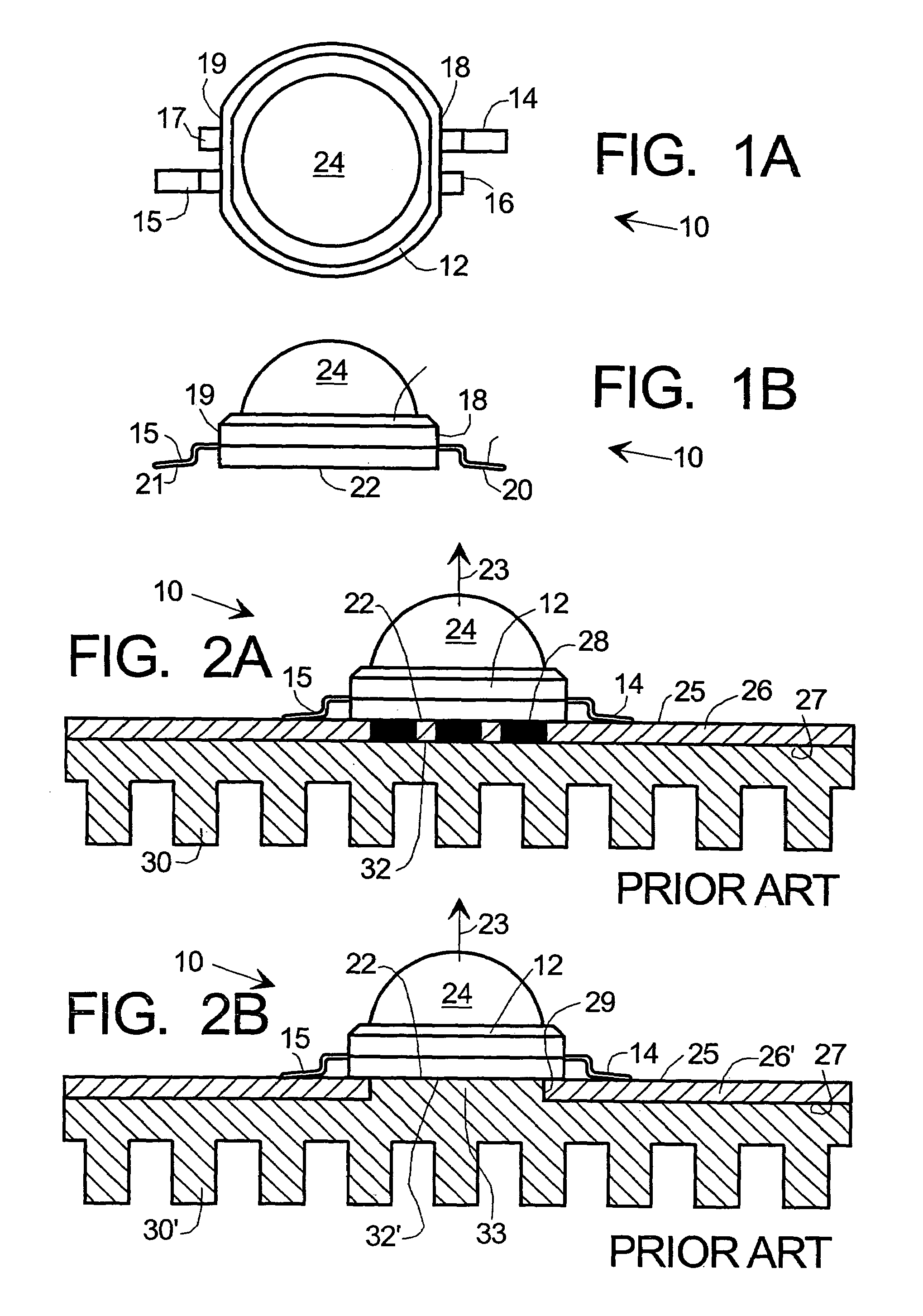
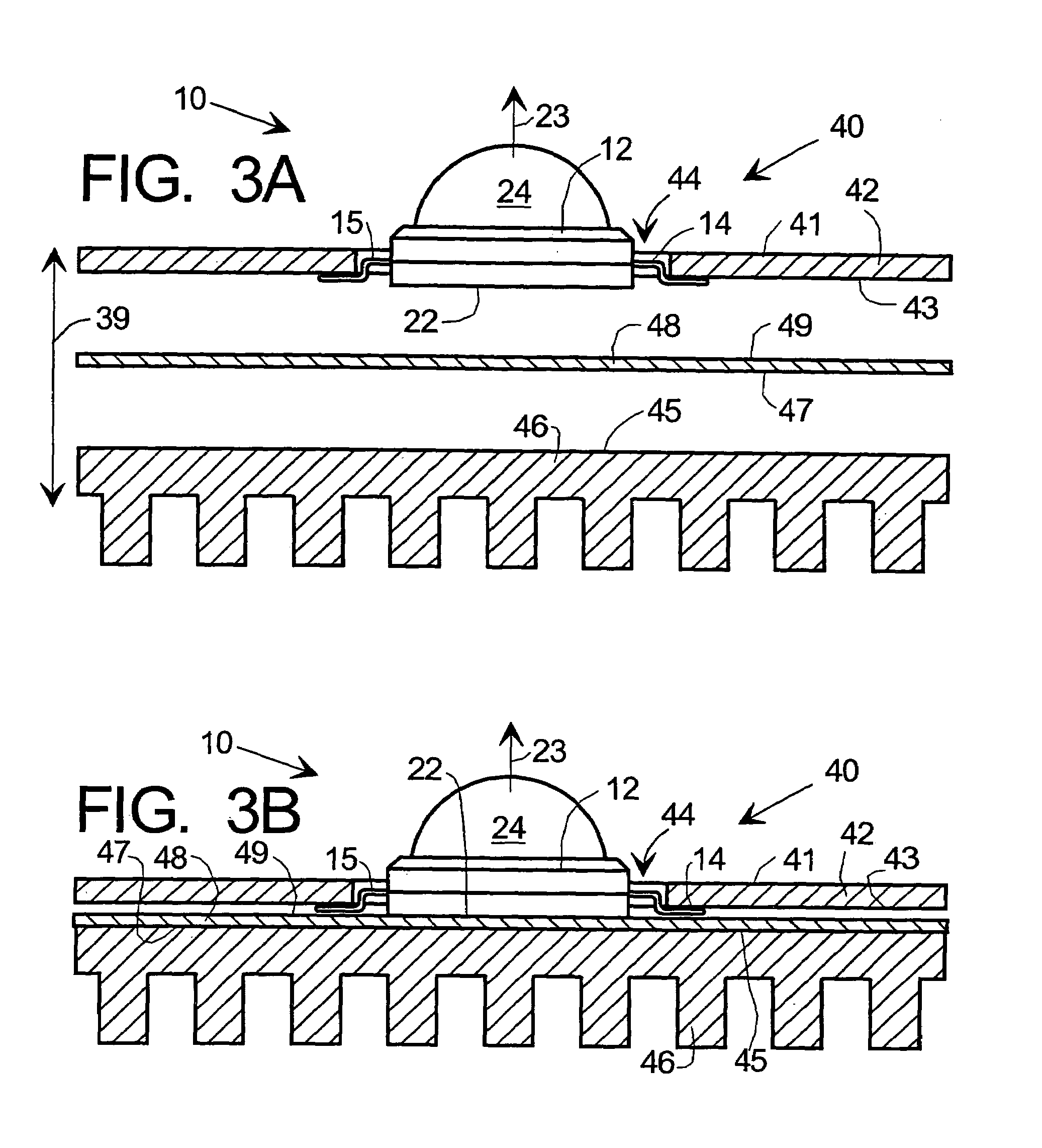
[0015]FIGS. 3A–B are partial cross-sectional views of arrangement 40 for mounting device 10 of FIGS. 1A–B on wiring board 42 and associated heatsink 46, according to the present invention, wherein FIG. 3A shows a partially assembled view (exploded in the direction of arrow 39) and FIG. 3B shows a fully assembled view. Arrangement 40 has device 10 of FIGS. 1A–B with leads 14–15, lens 24, package body 12 and lower heat dissipating surface 22. Leads 14–15 are attached (e.g., by soldering) to appropriate contact regions (not shown) on lower surface or underside 43 of PWB 42. PWB 42 has through-hole 44 for receiving body 12 of device 10. Lens 24 faces away from upper surface 41 of PWB 42 and from heatsink 46. Leads 14–15 are desirably formed such that when device body 12 is installed in through-hole 44 and leads 14–15 are attached to electrical contacts (not shown) provided on lower surface 43 of PWB 42, and that base 22 of package body 12 extends slightly below lower surface 43 of PWB 4...


PUM


Abstract

Method and apparatus are provided for thermally coupling one or more electronic devices to a heatsink. The apparatus comprises a heatsink having a substantially planar upper surface, a wiring board (PWB) with a through-hole for receiving the device such that a principal face thereof is in thermal contact with the heatsink, its electrical leads are captured between at least a portion of the wiring board and the heatsink, and a top of the device protrudes through the PWB. The method comprises placing the device in the through-hole with its base exposed on and protruding from the underside of the PWB, attaching its electrical leads to contacts on the wiring board and pressing the PWB toward the heatsink with the leads captured there between. An electrically insulating thermally conducting layer is desirably placed between the wiring board and the heatsink.

Description

TECHNICAL FIELD[0001]The present invention generally relates to improved heatsinking of electronic devices, and more particularly to heatsinking of relatively high power dissipation electronic devices having surface mount package configurations or equivalent.BACKGROUND[0002]Many modern day electronic devices are often enclosed in what are referred to as surface mount packages, that is, packages generally intended to sit on or above a wiring board and having leads formed in such a way as to readily attach (e.g., by soldering) to contact regions on the surface of the wiring board, as opposed to being inserted into contact holes passing through the wiring board. By way of illustration and not intended to be limiting, FIG. 1A is a top view and FIG. 1B is a side view of high power light emitting diode (LED) 10 having surface mount package 12. LED 10 in package 12 has electrical leads or contacts 14–17 protruding laterally from sides 18–19 of LED package 12. Leads 14–15 of package 12 are ...

Claims


Application Information

Patent Timeline
Patent Type & Authority Patents(United States)
IPC IPC(8): H05K7/20F21K99/00F21V29/00H01L25/13H01L33/00H05K1/02H05K1/18
CPCF21K9/00F21V29/004H05K1/021F21V29/763F21Y2101/02F21Y2105/001H05K3/0061H05K2201/10106H01L2924/0002H05K1/182H01L2924/00F21Y2105/10F21Y2115/10H01L23/34
Inventor NEWBY, THEODORE A.
Owner HONEYWELL INT INC
Why Eureka
Try Eureka