Method of producing active semiconductor layers of different thicknesses in an SOI wafer

a technology of active semiconductor and soi wafer, which is applied in semiconductor/solid-state device manufacturing, electric devices, solid-state devices, etc., can solve the problems of limited structural resolution, complex structure, and inability to dielectrically isolate vertical dmos transistor cells, and achieve high packing density, limited structural resolution, and high breakdown or breakthrough field strength

Active Publication Date: 2006-02-21
ATMEL GERMANY
View PDF12 Cites 99 Cited by
  • Summary
  • Abstract
  • Description
  • Claims
  • Application Information

AI Technical Summary

Benefits of technology

[0022]The inventive method enables a simultaneous integration of low power CMOS and high power DMOS (so-called “ultra smart power”) on regions or portions of active semiconductor material respectively having different thicknesses. Through the use of an SOI wafer, it is possible to integrate DMOS elements on a thick SOI substrate and CMOS elements on a thin SOI substrate using a common SOI technology on a single common wafer with maximum packing density. The active semiconductor material that is overgrown in the context of the inventive method has no connection to the substrate, so that a complete electrical decoupling or dielectric isolation of the thin active semiconductor layers from the substrate can be achieved. Another advantage of the invention is that the seed openings for the selective epitaxy are formed independent of lithographic processes, whereby space is saved and a higher integration density is achieved. Overall, the inventive method reduces an increase of leakage currents that are expected in connection with a scaled reduction of the structural width.
[0023]It is preferred according to the invention that the trench is produced by means of a shallow trench isolation (STI) etching technology, which involves an anisotropic etching process to form an etched trench between active regions that have been covered with a nitride protective layer, and then the trench is filled with an insulating material such as silicon dioxide or polysilicon. Thereby, the STI technology is able to achieve high packing densities.
[0024]It is further preferred that the step or process of producing spacers at the sides within the trench structure on the first oxide layer involves the following sub-steps: covering the trench including the inner wall areas of the trench with a polycrystalline semiconductor material, and then anisotropically etching away the polycrystalline semiconductor material from the central floor area of the trench, so that only spacers of the polycrystalline semiconductor material remain along the inner wall regions of the trench.
[0025]In view of the above, it is apparent that the material for the spacers is provided by the covering of the trench structure. Further in this regard, an etching process is regarded as anisotropic when the etching front progresses in a certain spatial direction more quickly than in other spatial directions. As a result of a more-rapid etching process in the vertical direction, thereby polycrystalline material will preferentially remain in place along the wall areas of the trench throughout and after the vertical anisotropic etching progresses vertically toward the trench floor. Thus, the remaining polycrystalline material along the trench sidewalls forms the desired poly-spacers. The width of the thusly produced poly-spacers will define the width of the seed openings to be formed in the trench for the following selective epitaxy. In this manner, it is possible to produce seed openings with nearly any desired arbitrarily small dimensions, for example also for technologies with a limited structural resolution. In this context, the term “seed” refers to the exposed surface structure of a monocrystal on which atoms will be deposited and begin to grow in the ELO process, such that the crystal material epitaxially grown in the ELO process will take on or mimic the crystal orientation of the seed crystal, i.e. the exposed surface of the underlying monocrystal.
[0026]According to a further preferred feature, the step of filling the trench with a second oxide layer between the spacers involves depositing a tetraethylorthosilicate (TEOS) oxide. In this regard, silicon dioxide is produced through the decomposition of the TEOS compound at moderate temperatures (e.g. up to about 700° C.). This process is also referred to as TEOS pyrolysis, and results in high-value, high-quality oxide films, which are characterized, for example, by a high breakdown or breakthrough field strength and a conforming edge covering ability.
[0027]It is also preferred that the step of covering the SOI wafer with a protective layer especially includes the following sub-steps: covering the SOI wafer with a first oxide partial layer; covering the first oxide partial layer with a nitride layer; and covering the nitride layer with a second oxide partial layer. This layering process sequence produces a so-called oxide-nitride-oxide (ONO) layer, which is used as a hard mask in the etching process for forming the trench. In comparison to a “soft” lacquer or resist mask, the use of such a hard mask achieves improved accuracy with which the angles and the shape of the sidewalls of the trench are produced. Moreover, during the later covering of the trench with an oxide layer, the nitride layer of the ONO multilayer prevents an undesired oxidation of areas of the surface of the layer of active semiconductor material lying outside of the trench.

Problems solved by technology

Furthermore, the vertical DMOS transistor cells are not dielectrically insulated relative to the substrate.
This a rather complicated and space-consuming structure.
This, however, is contrary to the requirements and demands for so-called smart-power-elements based on DMOS technology with high dielectric strength and good thermal dissipation.
However, the scaled reduction of size of components in BCDMOS circuits with vertical SOI insulation is limited by the above mentioned mutually contrary requirements.

Method used


Image

  • Method of producing active semiconductor layers of different thicknesses in an SOI wafer
  • Method of producing active semiconductor layers of different thicknesses in an SOI wafer
  • Method of producing active semiconductor layers of different thicknesses in an SOI wafer

Examples


Embodiment Construction

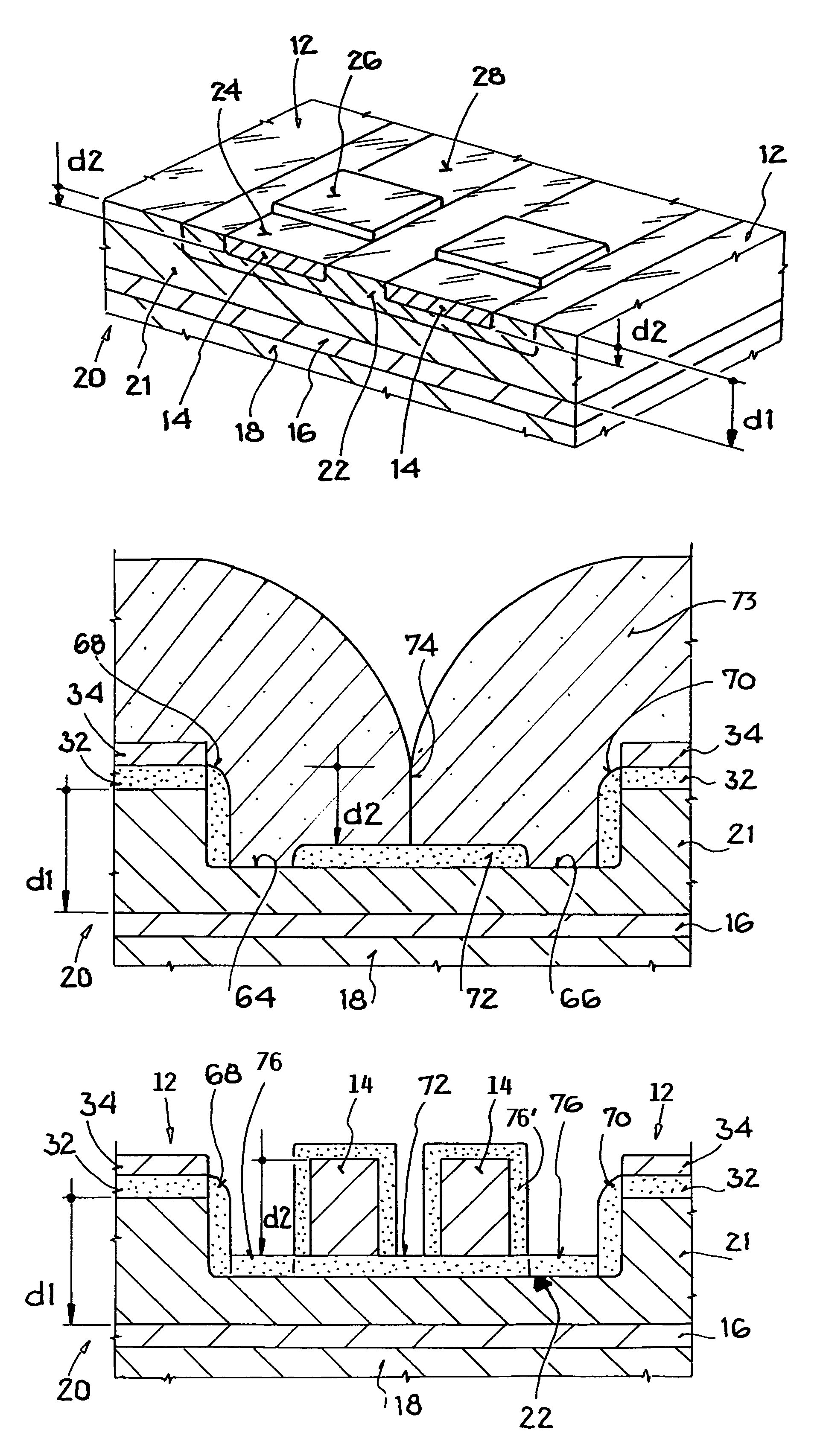
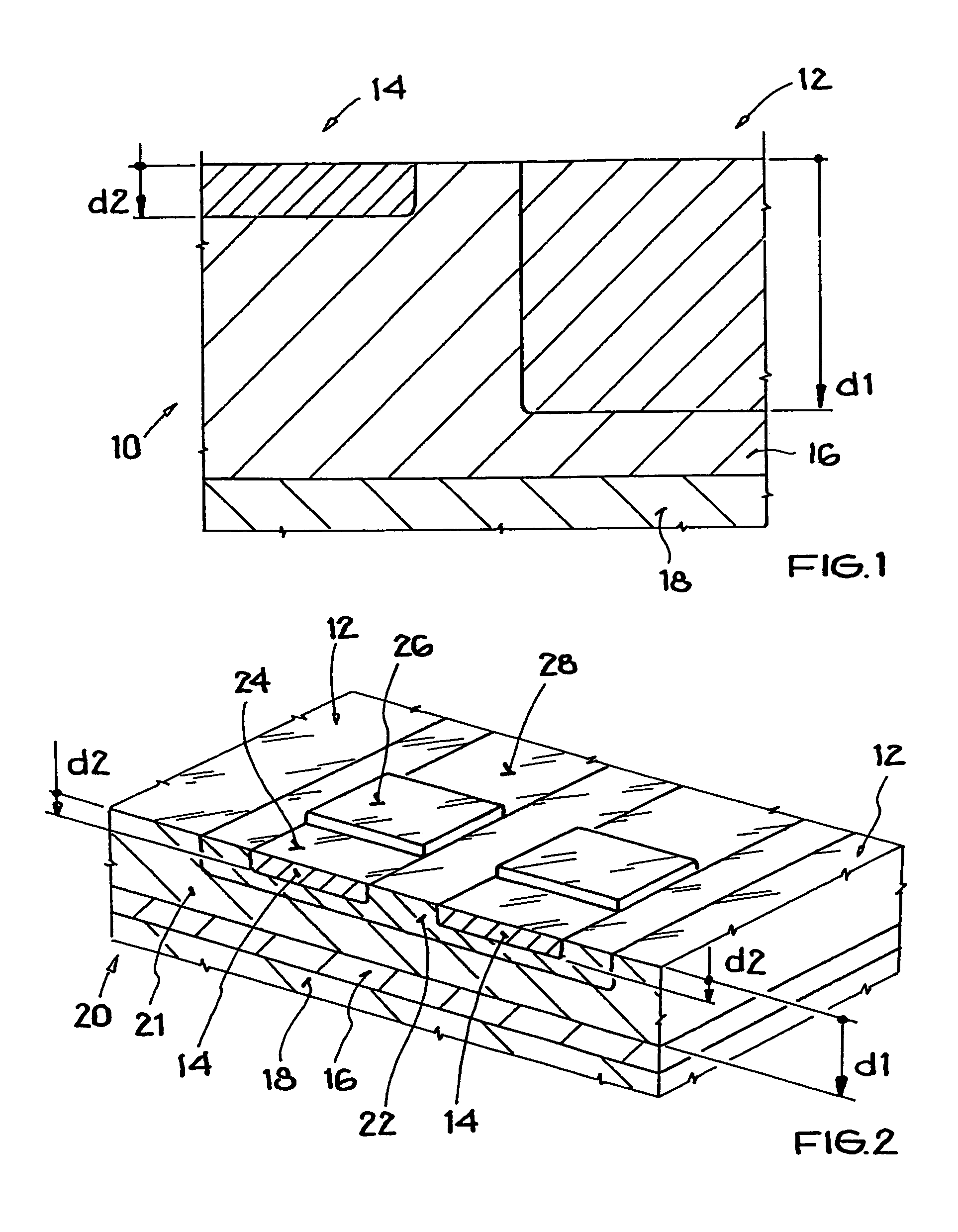
[0043]FIG. 1 shows a cross-section of a portion of an SOI wafer 10, which includes first and second active regions 12 and 14 of active semiconductor material, whereby these two regions respectively have different thicknesses. Namely, the first active region 12 has a comparatively large thickness d1, while the second active region 14 has a comparatively smaller thickness d2. The two active regions 12 and 14 are embedded in an insulating dielectric layer 16, which extends on an underlying handle or handling layer 18.

[0044]Due to its comparatively small thickness d2, the second active region 14 is especially well suited to the fabrication of CMOS elements. In order to avoid leakage currents and therewith power losses in the second active region 14, and in order to prevent parasitic capacitances, the thickness d2 should amount to 200 nm for example. On the other hand, the first active region 12 with its comparatively large thickness d1 is especially adapted or well suited to the fabrica...


PUM


Abstract

An SOI wafer including an active semiconductor material layer on an insulating layer is processed to form thereon first and second active semiconductor regions that respectively have different thicknesses and that are vertically and laterally insulated. In the process, a trench is etched into the SOI wafer, seed openings are formed in the bottom of the trench to reach the underlying active material layer, the trench is filled with epitaxially grown semiconductor material progressing from the seed openings, some of the epitaxially grown material is removed to form the second active regions, and oxide layers are provided so that the second active regions are laterally and vertically insulated from the first active regions formed by remaining portions of the active semiconductor material layer.

Description

PRIORITY CLAIM[0001]This application is based on and claims the priority under 35 U.S.C. §119 of German Patent Application 10 2004 005 506.8, filed on Jan. 30, 2004, the entire disclosure of which is incorporated herein by reference.FIELD OF THE INVENTION[0002]The invention relates to a method of producing insulated active semiconductor regions having different layer thicknesses in an SOI wafer including a layer of active semiconductor material on an insulating layer.BACKGROUND INFORMATION[0003]A conventional method pertinent to the above general field of the invention is known from U.S. Pat. No. 6,204,098, wherein dielectrically insulated islands are produced on an SOI substrate. The insulated islands are filled by epitaxially grown material, whereby the active silicon layer of the SOI wafer serves as a seed for the growth. Through such a process, only insulated islands having the same height or thickness can be produced. An active layer within these islands has a first relatively ...

Claims


Application Information

Patent Timeline
Patent Type & Authority Patents(United States)
IPC IPC(8): H01L21/84H01L21/762H01L27/12
CPCH01L21/76264H01L27/1203H01L21/84
Inventor DIETZ, FRANZDUDEK, VOLKERGRAF, MICHAEL
Owner ATMEL GERMANY
Why Eureka
Try Eureka