Semiconductor integrated circuit

Active Publication Date: 2006-02-28
SOCIONEXT INC
View PDF6 Cites 2 Cited by
  • Summary
  • Abstract
  • Description
  • Claims
  • Application Information

AI Technical Summary

Benefits of technology

[0018]In the present invention, the intervals between the cells forming the second group of cells are wider than those between the cells forming the first group of cells, so that wiring congestion in a wiring region of an innerly disposed group of cells can be eliminated. Further, when the number of the cells forming the second group of cells is made less than that of the cells forming the first group of cells, the size o

Problems solved by technology

For example, in the case of a wire 713, wiring is impractical because there is no wiring channel remaining.
Further, as is the case with the wire region 712, the more innerly a group of cells is located, the more congested the wiring is, becoming more susceptible to crosstalk.
In the worst case thereof, a required performance cannot be achieved.
However, since the more in

Method used


Image

  • Semiconductor integrated circuit
  • Semiconductor integrated circuit
  • Semiconductor integrated circuit

Examples


Example

[0027]First Embodiment

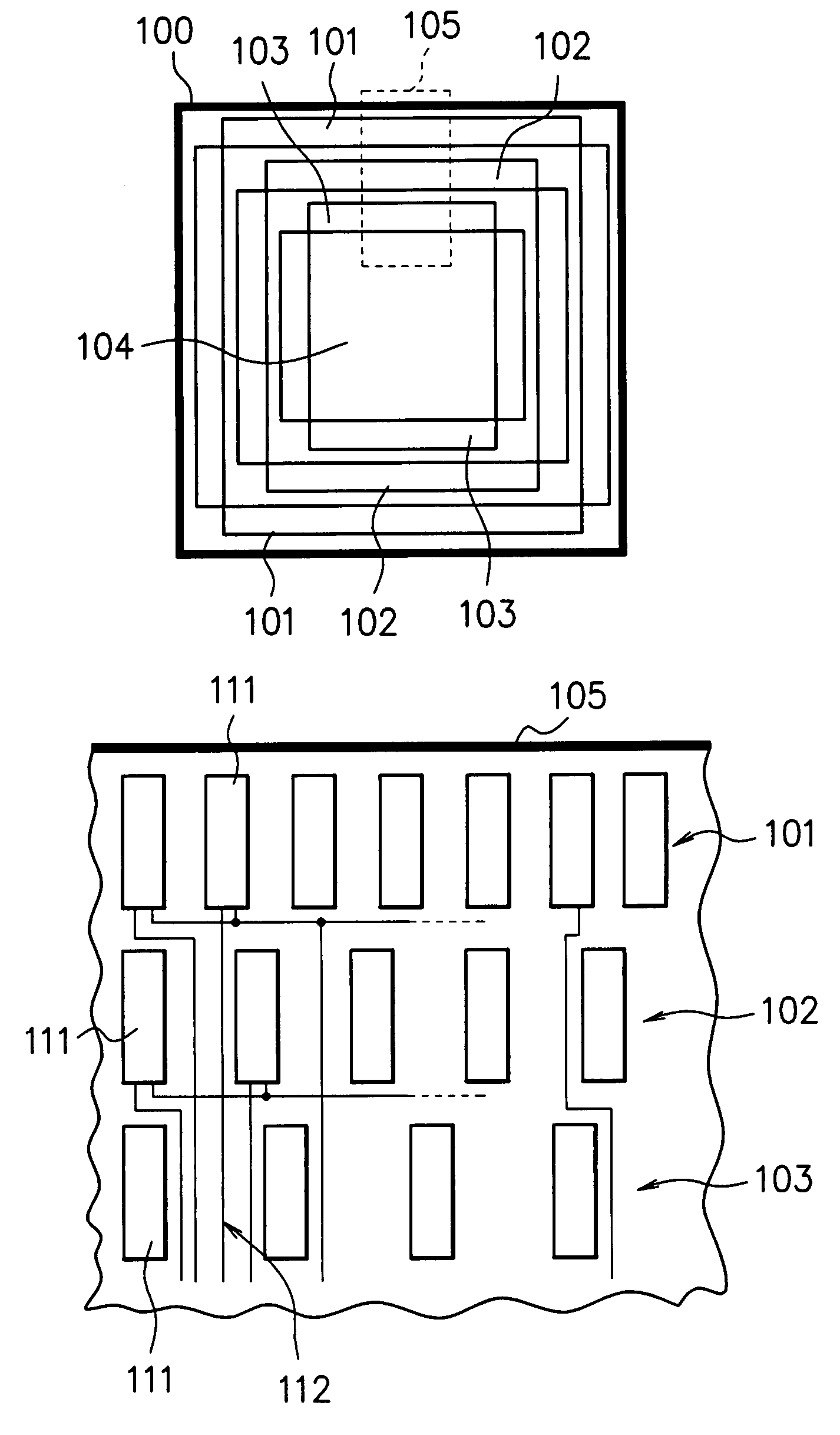
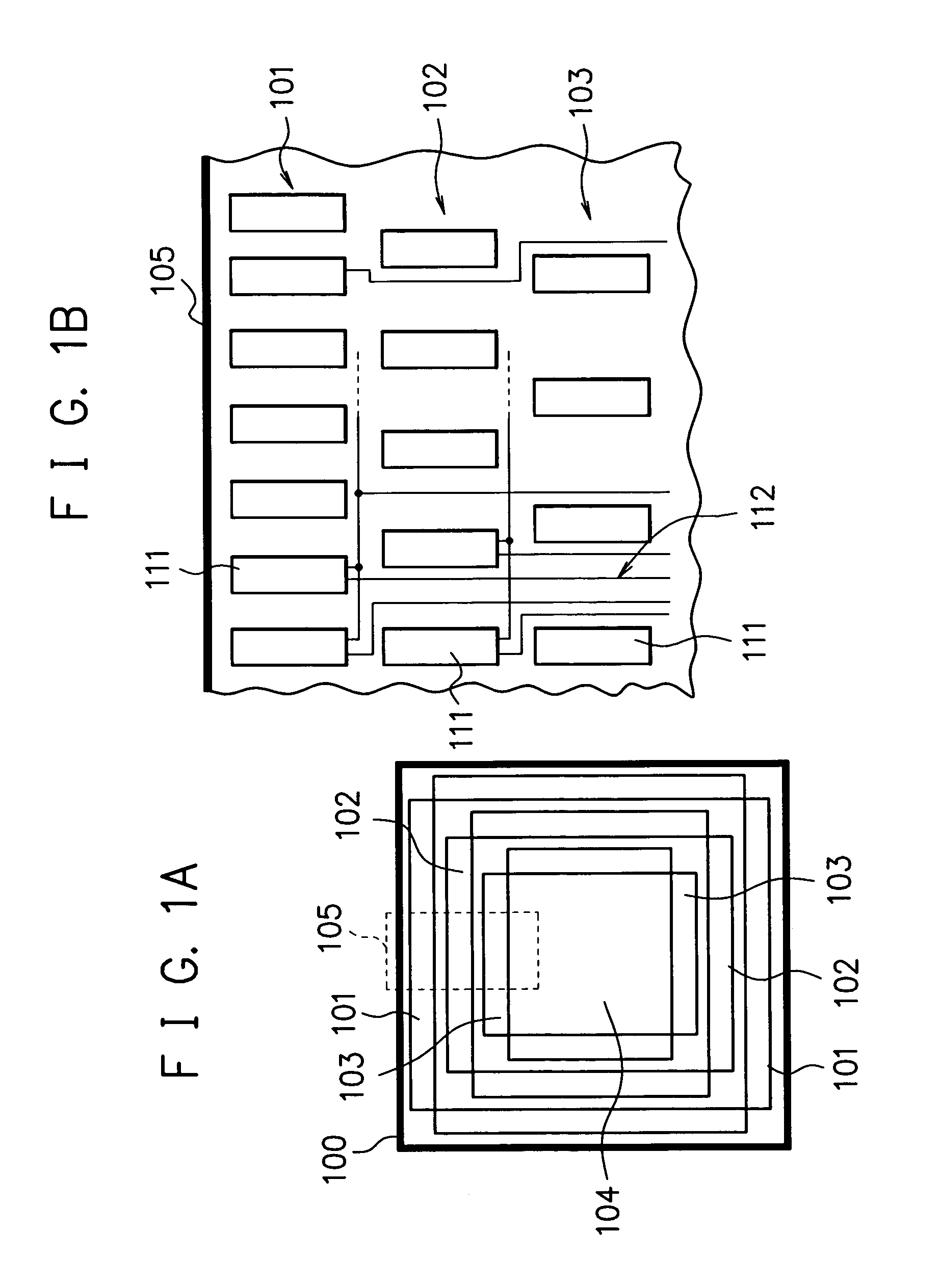
[0028]FIGS. 1A and 1B show a semiconductor integrated circuit in which I / O cells and / or power source cells configured in multistage are arranged according to a first embodiment of the present invention.

[0029]FIG. 1A shows a configuration of a semiconductor integrated circuit (semiconductor chip) 100. The semiconductor integrated circuit 100 includes a first group of cells 101, a second group of cells 102, and a third group of cells 103, along the circumferential frame region thereof, and innerly disposed circuit cells in an internal region 104 thereof. In each of the first to third groups of cells 101 to 103, respective plural I / O cells are arranged annularly along a direction of the outer periphery. The first group of cells 101, the second group of cells 102, and the third group of cells 103 are, respectively, the outermost group of cells, the second outermost group of cells, and the third outermost group of cells, in the semiconductor integrated circuit 100.

[...

Example

[0034]Second Embodiment

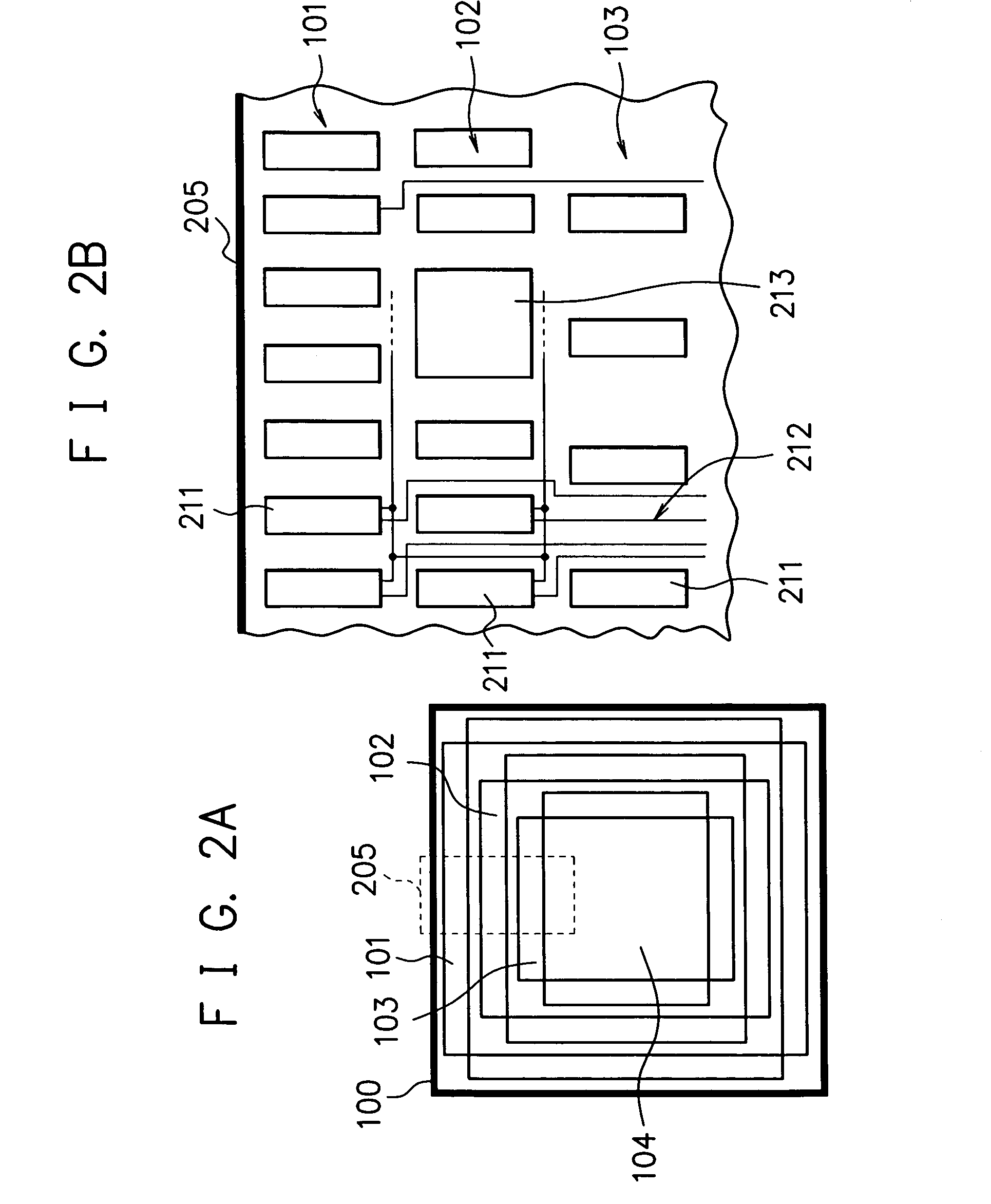
[0035]FIGS. 2A and 2B show a semiconductor integrated circuit in which I / O cells and / or power source cells configured in multistage are arranged according to a second embodiment of the present invention.

[0036]FIG. 2A shows a configuration of a semiconductor integrated circuit 100 which is equivalent to that of the first embodiment as shown in FIG. 1A. FIG. 2B is an enlarged view of a region 205 which is a part of the semiconductor integrated circuit shown in FIG. 2A. The region 205 includes a first group of cells 101, a second group of cells 102, and a third group of cells 103. It is a configuration in which the groups of cells are arranged in three stages, and cells of two different sizes, cells 211 and 213, are included. In the first group of cells 101, the cells 211 of a uniform size are arranged. The second group of cells 102 includes a number of cells 211 among which small number of the cells 213 which are larger than the cells 102 in size exist. Dependin...

Example

[0041]Third Embodiment

[0042]FIGS. 3A and 3B show a semiconductor integrated circuit in which I / O cells and / or power source cells configured in multistage are arranged according to a third embodiment of the present invention.

[0043]FIG. 3A shows a configuration of a semiconductor integrated circuit 100 which is equivalent to that of the first embodiment shown in FIG. 1A. Over the semiconductor integrated circuit 100, area bumps (metal bumps) 306 are provided, which are two-dimensionally arranged.

[0044]FIG. 3B is an enlarged view of a region 305 which is a part of the semiconductor integrated circuit shown in FIG. 3A. The region 305 includes a first group of cells 101, a second group of cells 102, and a third group of cells 103. In each of the groups of cells 101 to 103, plural I / O cells and / or power source cells 111 are arranged whose sizes are uniform for each group of cells as in the first embodiment shown in FIG. 1B. The area bumps 306 disposed over the semiconductor integrated cir...


PUM


Abstract

A semiconductor integrated circuit is provided, which includes a first group of cells, in which a plural of I/O cells and/or power source cells for external input and/or output are arranged along a direction of the outer periphery of the semiconductor integrated circuit, and a second group of cells on an inner side of the first group of cells in which a plural of I/O cells and/or power source cells for external input and/or output are arranged along a direction of the outer periphery of the semiconductor integrated circuit. The intervals between the cells forming the second group of cells are wider than those between the cells forming the first group of cells.

Description

CROSS-REFERENCE TO RELATED APPLICATIONS[0001]This application is based upon and claims the benefit of priority from the prior Japanese Patent Application No. 2003-059834, filed on Mar. 6, 2003, the entire contents of which are incorporated herein by reference.BACKGROUND OF THE INVENTION[0002]1. Field of the Invention[0003]This invention relates to a semiconductor integrated circuit and, more particularly, to a semiconductor integrated circuit having input / output (I / O) cells and / or power source cells.[0004]2. Description of the Related Art[0005]In a semiconductor integrated circuit, I / O cells are often arranged in multistage in order to cope with the multiplication of pins. The arrangement intervals for I / O cells in a multistage configuration are such that both outer I / O cells and inner I / O cells are arranged at predetermined intervals.[0006]FIGS. 7A and 7B show a semiconductor integrated circuit having a configuration in which I / O cells are arranged in multistage according to a firs...

Claims


Application Information

Patent Timeline
IPC IPC(8): H03K19/177H01L27/04G11C5/02H01L21/82H01L21/822
CPCG11C5/025H01L2224/73265H01L2224/48091H01L2924/00014
Inventor ANAZAWA, TETSUYA
Owner SOCIONEXT INC
Why Eureka
Try Eureka