
Image input apparatus

a technology of input apparatus and image, which is applied in the field of image input apparatus, can solve the problems of reducing the number of units, so as to achieve the effect of simple construction

Inactive Publication Date: 2006-03-07
MINOLTA CO LTD +1
View PDF11 Cites 148 Cited by
  • Summary
  • Abstract
  • Description
  • Claims
  • Application Information

AI Technical Summary

Benefits of technology

[0013]An object of the present invention is to provide an image input apparatus that has a simple construction, that is more compact than ever, and that offers high-resolution images.

Problems solved by technology

However, it is impossible to miniaturize beyond a certain limit such apparatuses by making their constituent components smaller, and therefore, to realize apparatuses so compact as to be portable all the time, it is necessary, and in fact expected, to develop a compact image input apparatus based on a novel construction.
H5-100186 mentioned above both have basically the same optical system, and suffer from unsatisfactory resolution in the image signals obtained.
However, even a microlens needs to have a certain size to function satisfactorily as a lens, and therefore, in this compound-eye optical system, it is impossible to increase beyond a certain limit the number of units even if the microlens are arranged in a closest packed structure.
As a result, it is difficult to obtain a high-resolution image.
H10-107975 mentioned above solves the problem of unsatisfactory resolution in the image signals obtained, but, to obtain the best optical characteristics in this optical system, it is necessary to arrange the microlens array and the photosensitive element array on a spherical surface having its center at the aperture stop, and thus this arrangement is not fit for the purpose of making the entire image input apparatus satisfactorily compact.
This makes the photosensitive elements difficult to arrange in desired positions, and thus makes the entire image input apparatus difficult to manufacture.
However, here, to prevent interference between the optical signals from adjacent microlenses, the photosensitive element array needs to be arranged at a certain distance from the microlens array, and thus the photosensitive element array requires an unduly large fitting area.
In addition, this arrangement is specialized for narrow object angles at the cost of optical characteristics, and therefore exhibits various drawbacks in practical use.

Method used


Image

  • Image input apparatus
  • Image input apparatus
  • Image input apparatus

Examples


Embodiment Construction

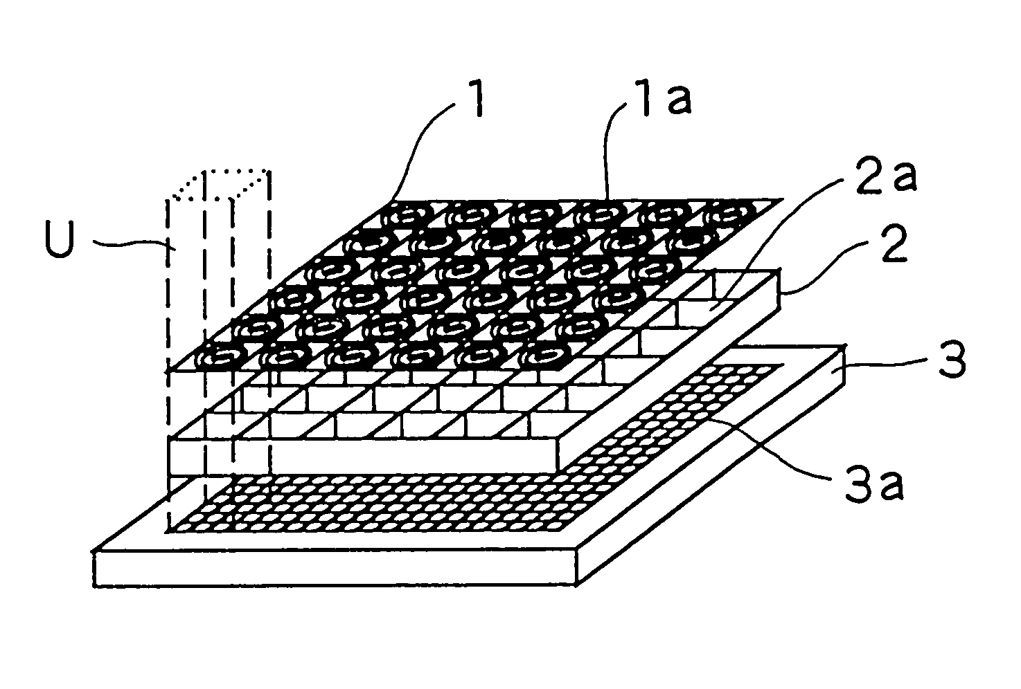
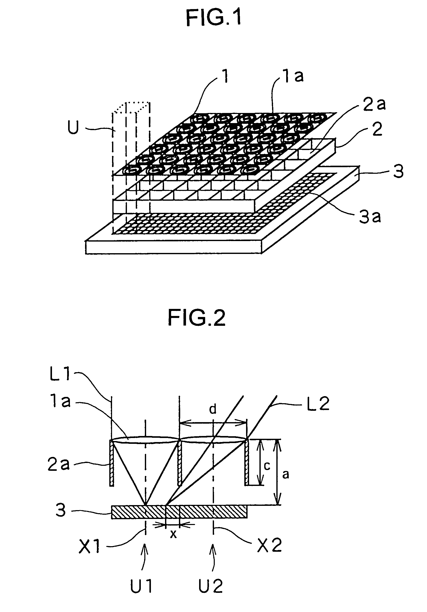
[0031]Hereinafter, embodiments of the present invention will be described with reference to the drawings. This invention provides a slim type image input apparatus in which a single plane photosensitive element array is divided into areas each corresponding to one microlens so that each area includes a plurality of photosensitive elements, and in addition partition walls are provided to prevent interference among the optical signals from the individual microlenses. FIG. 1 is an exploded perspective view schematically showing an image input apparatus embodying the invention.

[0032]In FIG. 1, reference numeral 1 represents a microlens array having microlenses 1a arranged in a two-dimensional array, in a square shape for example, and reference numeral 3 represents a photosensitive element array disposed below the microlens array 1 so as to face it and having photosensitive elements 3a arranged similarly in a two-dimensional array, in a square shape for example. Reference numeral 2 repre...


PUM


Abstract

An image input apparatus has a photoelectric converter element having a flat photosensitive surface and an image formation unit array having a plurality of image formation units arranged in an array. This image formation units individually receive light beams substantially from an identical area and focus the received light beams on different regions of the photosensitive surface of the photoelectric converter element to form images thereon.

Description

[0001]This application is based on application No. H11-233760 filed in Japan on Aug. 20, 1999, the entire contents of which are hereby incorporated by reference.BACKGROUND OF THE INVENTION[0002]1. Field of the Invention[0003]The present invention relates to an image input apparatus that forms an image through a plurality of minute-image-formation optical systems.[0004]2. Description of the Prior Art[0005]In recent years, with the advent of highly information-oriented society brought by the development of communications media, there has been a keen demand for acquiring various kinds of information effectively and timely. Such information includes a very large proportion of image information, and therefore recording and saving of image information are essential for conducting advanced information processing activities. Conventionally, apparatuses such as photographic cameras and video cameras have been used for recording and saving image information. However, it is impossible to minia...

Claims


Application Information

Patent Timeline
IPC IPC(8): H04N5/225G02B3/00G06T1/00H04N1/19H04N5/335H04N5/372H04N9/07H04N13/02
CPCH01L27/1462H04N5/335H01L27/14683H04N5/2254H01L27/14627G02B3/0018G02B3/0056H01L27/14685H04N25/00
Inventor TANIDA, JUNYAMADA, KENJIMIYAZAKI, DAISUKEICHIOKA, YOSHIKIMIYATAKE, SHIGEHIROISHIDA, KOUICHI
Owner MINOLTA CO LTD
Learn More