IC with internal interface switch for testability

a technology of testability and internal interface, which is applied in the field of testing techniques in semiconductor integrated circuits, can solve the problems of a large number of test patterns and a lower failure detection ratio, and achieve the effect of reducing the developing period of a semiconductor integrated circuit and increasing flexibility

Inactive Publication Date: 2006-03-14
RENESAS ELECTRONICS CORP +1
View PDF35 Cites 25 Cited by
  • Summary
  • Abstract
  • Description
  • Claims
  • Application Information

AI Technical Summary

Benefits of technology

[0014]The bus interface circuit converts the levels of input/output signals in accordance with specifications of the semiconductor integrated circuit, sets timings, and controls a communication protocol. In conventional semiconductor integrated circuits, a test interface circuit of different specifications has been designed for each semiconductor integrated circuit, whereas according to the means mentioned above, it is unnecessary to design a test interface circuit of different specifications for each semiconductor integrated circuit. Further, with respect to a scan path, only a path is required for connecting the input/output terminals of each function module to the external interface switching circuit during a test operation. For this reason, either a scan path or a te

Problems solved by technology

However, for a large scale logical integrated circuit, this method requires an i

Method used


Image

  • IC with internal interface switch for testability
  • IC with internal interface switch for testability
  • IC with internal interface switch for testability

Examples


Embodiment Construction

[0026]In the following, preferred embodiments of the present invention will be described with reference to the drawings.

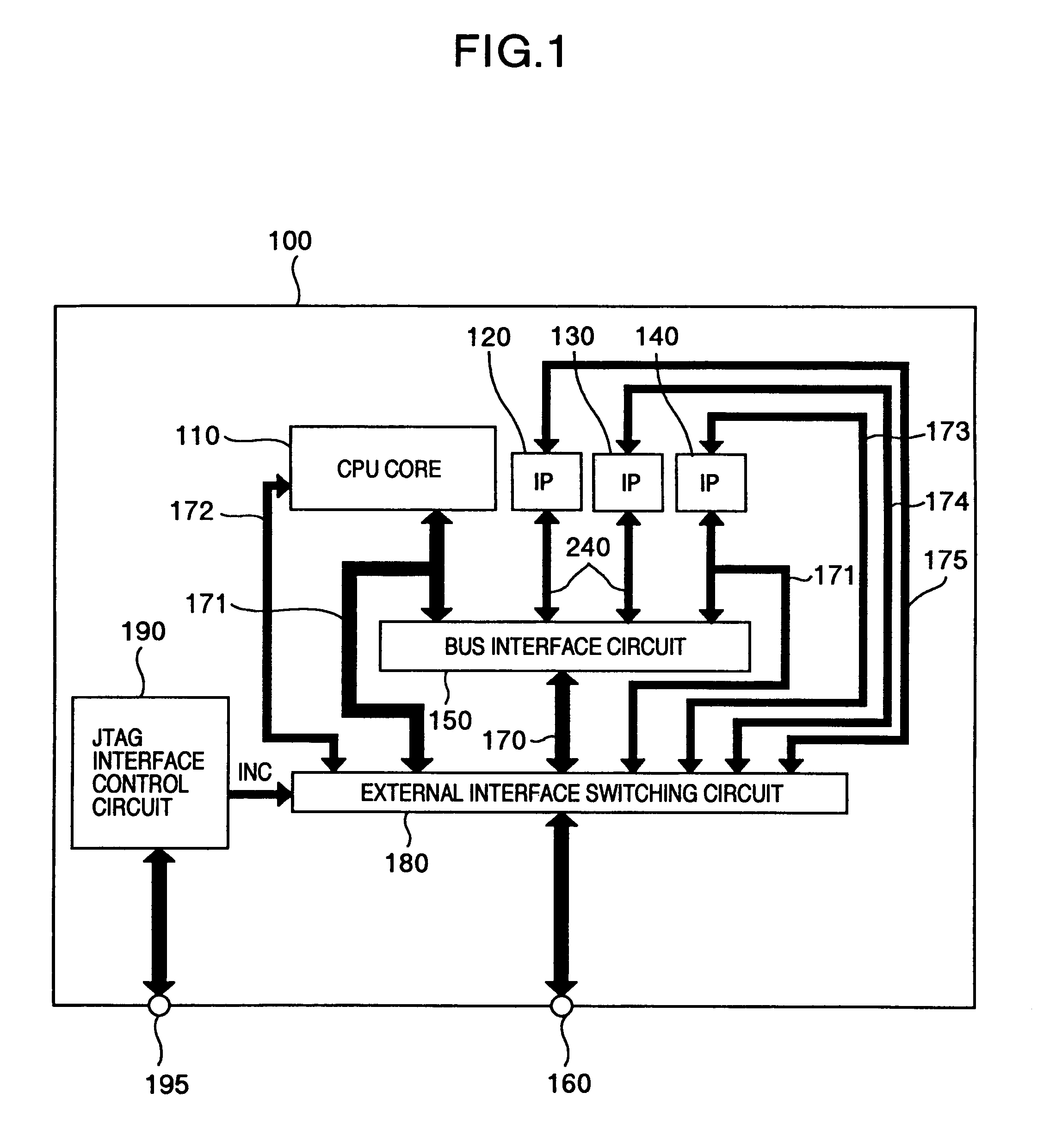
[0027]FIG. 1 is a block diagram of one embodiment of a system LSI as an exemplary semiconductor integrated circuit to which the present invention is applied, wherein the system LSI is fabricated on a single semiconductor chip 100 such as a single crystal silicon by known semiconductor integrated circuit manufacturing technologies.

[0028]FIG. 1 illustrates, as an exemplary system LSI, a general configuration of a microprocessor or a single-chip microcomputer to which the present invention is applied.

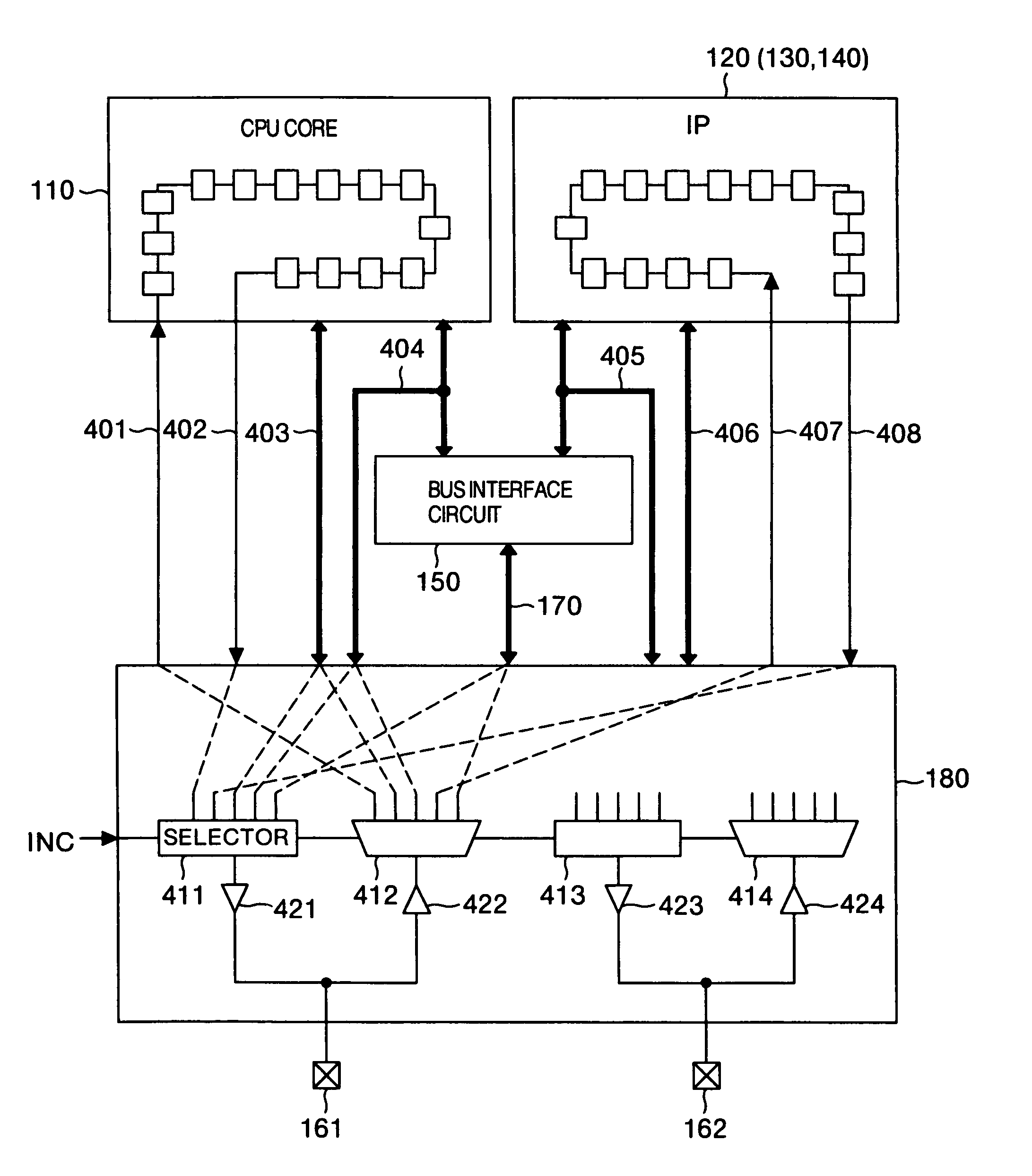
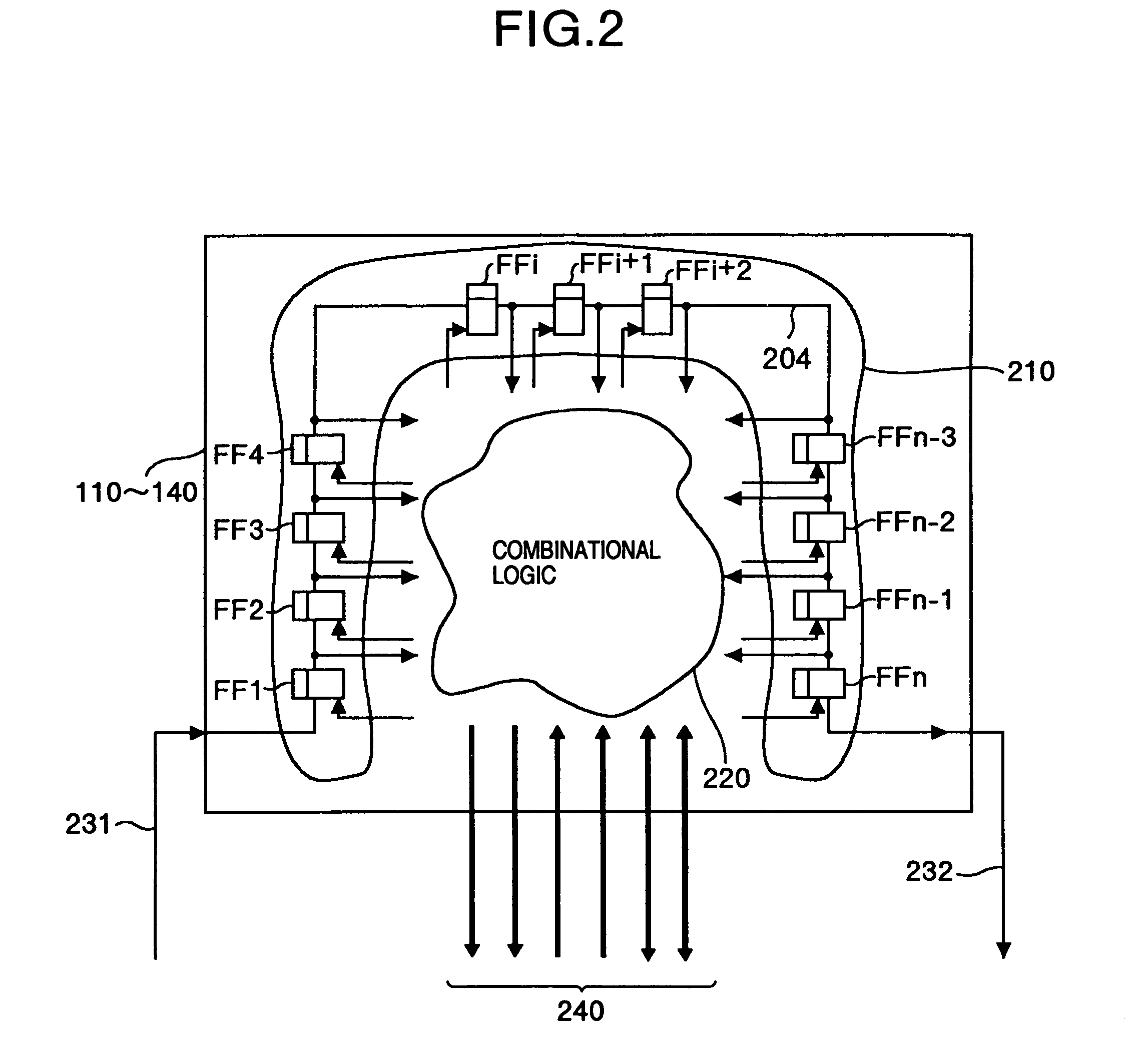
[0029]Reference numerals 110–140 in FIG. 1 designate function modules which are formed on the semiconductor chip 100 and constitute a system having desired functions; 150, a bus interface circuit for inputting / outputting signals between these modules and external devices provided external to the semiconductor chip 100; and 160, a plurality of external terminals for inputt...


PUM


Abstract

A semiconductor integrated circuit which is provided with a shift scan path incorporated in each function module and a testing I/O terminal connected to a shift scan path and provided separately from a normal-operation-use I/O terminal, and which comprises, all formed on one semiconductor chip, a bus interface circuit for connecting normal-operation-use I/O terminals of a plurality of function modules to a bus, an external interface switching circuit which switches between the bus-side I/O terminal of the bus interface circuit and the testing I/O terminal of each function module for connection to an external terminal and an interface control circuit for switch-controlling the external interface switching circuit.

Description

TECHNICAL FIELD[0001]The present invention relates to testing techniques in semiconductor integrated circuits (IC: Integrated Circuit), and more particularly to techniques which are effectively applied to testing systems for system LSIs (Large Scale Integration) such as a data processing unit composed of a plurality of function modules, a microprocessor, and a single-chip microcomputer.BACKGROUND ART[0002]With the advancement of micro-machining technologies, an increasingly larger logical scale of semiconductor integrated circuit can be fabricated on a single semiconductor chip. For this reason, there have been provided semiconductor integrated circuits which have systematic functions fabricated on a single semiconductor chip such as a microprocessor and a single-chip microcomputer (hereinafter also called the “system LSI”), which have conventionally been implemented by a plurality of chips.[0003]When a circuit having a variety of functions such as a central processing unit (CPU), a...

Claims


Application Information

Patent Timeline
IPC IPC(8): G01R31/28G01R31/3185G06F11/267
CPCG01R31/318558G06F11/2236G11C29/48G01R31/318572G01R31/318541G01R31/318555G11C2029/3202
Inventor KAMEI, TATSUYANISHIMOTO, JUNICHITATEZAWA, KEN
Owner RENESAS ELECTRONICS CORP
Why Eureka
Try Eureka