Double gate field effect transistor and method of manufacturing the same

a field effect transistor and double gate technology, applied in the field of semiconductor devices, can solve the problems of short distance between a source region and a drain region, interference with each other, and affect the channel region,

Inactive Publication Date: 2006-03-21
SAMSUNG ELECTRONICS CO LTD
View PDF14 Cites 34 Cited by
  • Summary
  • Abstract
  • Description
  • Claims
  • Application Information

AI Technical Summary

Benefits of technology

[0011]Embodiments of the invention provide a double gate field effect transistor formed on a bulk silicon substrate, in which the number of fins may be controlled, where two gates are self aligned to each other and a source and a drain region are also self aligned, and where a channel resistance may be reduced.
[0012]Other embodiments of the invention provide a method of manufacturing a double gate field effect transistor that uses a bulk silicon substrate, which can control a number of fins as required, has two gates formed by self aligning, and fins and STI films are also self aligned, having thereby a decreased channel resistance.

Problems solved by technology

However, a few problems associated with a reduction of channel length below 100 nm are observed in a conventional MOSFET that includes a planarized transistor.
An exemplary problem in this respect is the short distance between a source region and a drain region in the MOSFET.
If the source region is too close to the drain region, they interfere with each other and affect, the channel region.
As a result, a device characteristic, i.e., an active switching function, which controls the operation of the transistor by controlling the gate voltage of the MOSFET is seriously degraded.
The SCE could degrade the electrical characteristics of the MOSFET, such as instability of sub-threshold voltage.
However, this method has some drawbacks since it requires high cost and a long process time for forming the solid epitaxy layer.
Also, patterning the channel and source and drain regions to a desired shape is not easy.

Method used


Image

  • Double gate field effect transistor and method of manufacturing the same
  • Double gate field effect transistor and method of manufacturing the same
  • Double gate field effect transistor and method of manufacturing the same

Examples


Embodiment Construction

[0017]Hereinafter, the invention will be described more fully with reference to the accompanying drawings in which preferred embodiments of the invention are shown. This invention may, however, be embodied in many different forms and should not be construed as being limited to the embodiments set forth herein. Rather, these embodiments are provided so that this disclosure is thorough and complete, and fully conveys the concept of the invention to those skilled in the art. In the drawings, the thickness of layers and regions are exaggerated for clarity. To facilitate understanding, identical reference numerals have been used, where possible, to designate identical elements that are common to the figures.

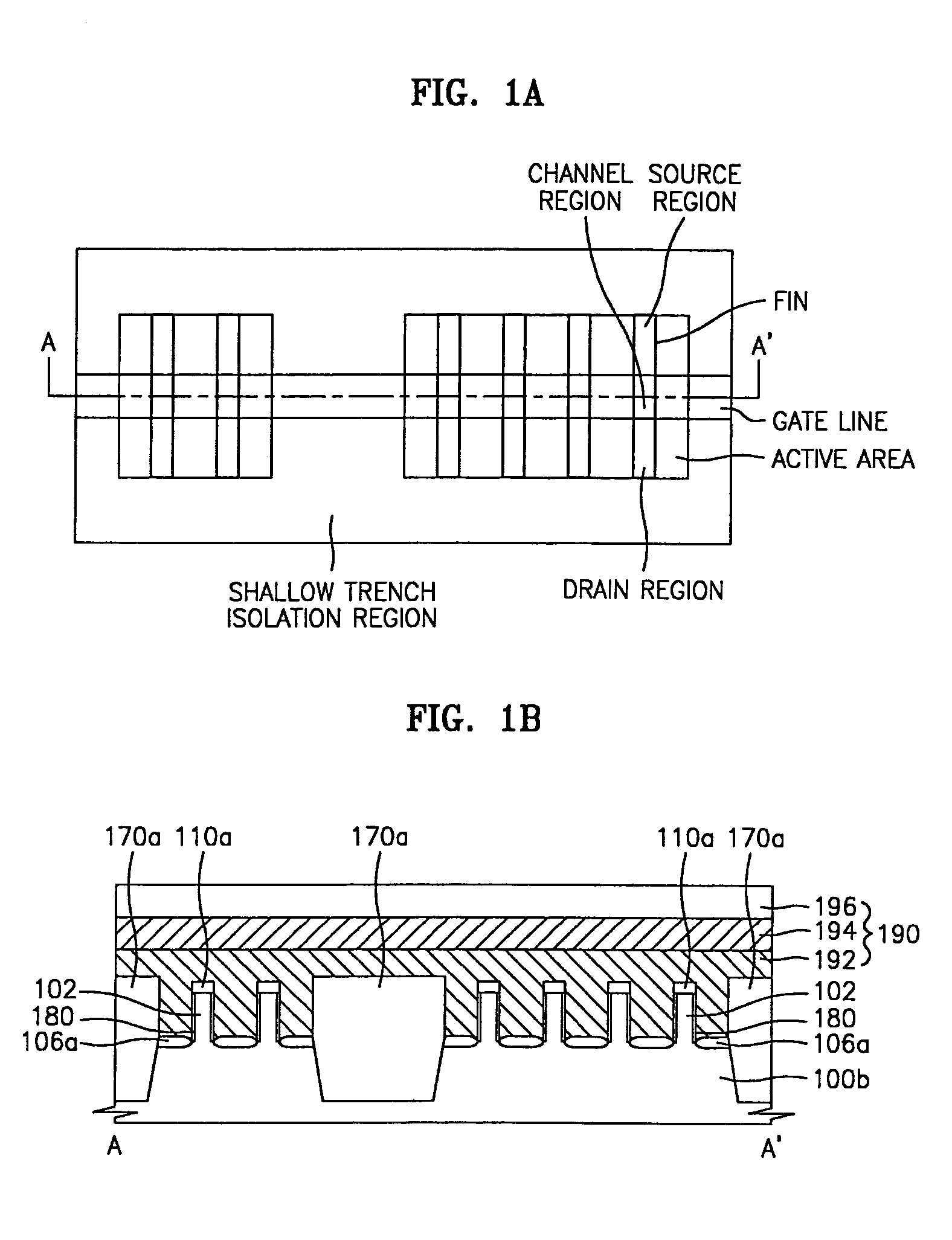
[0018]FIG. 1A is a plan diagram illustrating a double gate field effect transistor according to some embodiments of the invention.

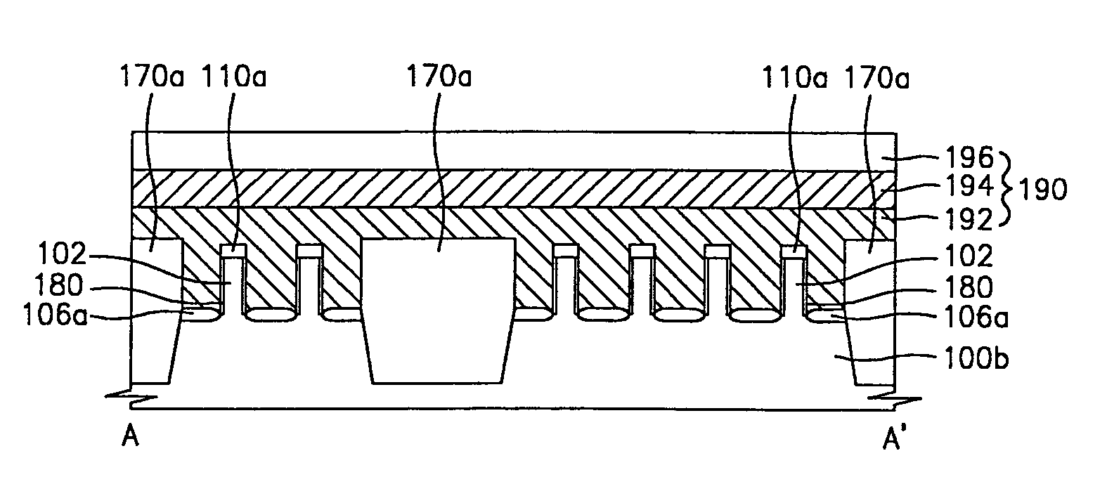
[0019]FIG. 1B is a cross-sectional diagram along line A–A′ in FIG. 1A.

[0020]Referring to FIGS. 1A and 1B, an active region is defined by shallow trench iso...


PUM


Abstract

Provided is a double gate field effect transistor and a method of manufacturing the same. The method of manufacturing the double gate field effect transistor comprises forming as many fins as required by etching a silicon substrate, masking the resultant product by an insulating material such as silicon nitride, forming trench regions for device isolation and STI film by using the silicon nitride mask, forming gate oxide films on both faces of the fins after removing the hard mask, and forming a gate line. As such, unnecessary channel formation under the silicon oxide film, when a voltage higher than a threshold voltage is applied to the substrate, is prevented by forming a thick silicon oxide film on the substrate on which no protruding fins are formed.

Description

CROSS REFERENCE TO RELATED APPLICATIONS[0001]This application claims priority from Korean Patent Application No. 2003-64153, filed on Sep. 16, 2003 in the Korean Intellectual Property Office, the disclosure of which is incorporated by reference in its entirety for all purposes.BACKGROUND OF THE INVENTION[0002]1. Field of the Invention[0003]This disclosure relates to a semiconductor device and a method of manufacturing the same, and more particularly, to a double gate field effect transistor formed on a bulk substrate and a method of manufacturing the same.[0004]2. Description of the Related Art[0005]As the integration density of a semiconductor device increases, the size of a metal-oxide-semiconductor field effect transistor (MOSFET) is miniaturized. For a semiconductor device having a planarized transistor, the miniaturization of a transistor corresponds to a reduction in a channel length of the transistor, thereby improving the performance characteristics, such as an operating spe...

Claims


Application Information

Patent Timeline
Patent Type & Authority Patents(United States)
IPC IPC(8): H01L21/336H01L21/00H01L21/338H01L27/092H01L21/8234H01L21/84H01L27/12H01L29/786
CPCH01L21/823437H01L21/823481H01L29/7851H01L27/1203H01L29/66795H01L21/84H01L27/092
Inventor YOON, JAE-MANPARK, DONG-GUNJIN, GYO-YOUNGMAKOTO, YOSHIDAPARK, TAI-SU
Owner SAMSUNG ELECTRONICS CO LTD
Why Eureka
Try Eureka