Split source RF MOSFET device

a technology of mosfet and split source, which is applied in the direction of movable seats, chairs, transportation and packaging, etc., can solve the problems of reducing gain, affecting ac output conductance and ac output capacitance of transistors, and less efficient operation of transistors in some applications, so as to reduce backgate modulation of channel regions

Inactive Publication Date: 2006-03-21
GATX VENTURES +1
View PDF3 Cites 5 Cited by
  • Summary
  • Abstract
  • Description
  • Claims
  • Application Information

AI Technical Summary

Benefits of technology

[0006]The present invention further provides for an integrated circuit having a circuit block having input and output terminals each having AC signals at an RF frequency and, at least, one RF MOS transistor connected to the circuit block. The RF MOS transistor has a plurality of drain regions elongated and parallel in the semiconductor substrate of the integrated circuit, a plurality of source regions elongated in the semiconductor substrate parallel to and interdigitated with the drain regions, a plurality of elongated gate electrodes over the semiconductor substrate defining channel regions separating the elongated drain regions from the elongated source regions, and a plurality of elongated tap regions in the semiconductor substrate that are parallel to and interdigitated with the elongated drain and source regions. Drain regions are connected to each other in parallel by a drain terminal that is coupled to a first power supply. The source regions are connected to each other in parallel by a source terminal that is coupled to an RF ground; the gate electrodes are connected to each other in parallel to a gate terminal that is connected to the circuit block input terminal. The tap regions are connected to the source regions locally. The tap regions provide an electrical voltage reference for the channel regions and are arranged so that each elongated source region is contiguous to an elongated tap region so that backgate modulation of the channel regions is reduced.

Problems solved by technology

However, at high frequencies the transistors operate less efficiently in some applications.
The AC output conductance and the AC output capacitance of the transistor are adversely affected.
An increase in output conductance results in reduced gain and bias dependency results in added distortion.
Additionally, in a low-noise amplifier circuit, unintended and undesirable circuit feedback voltage may be induced from the back gate-to-source connection.

Method used


Image

  • Split source RF MOSFET device
  • Split source RF MOSFET device
  • Split source RF MOSFET device

Examples


Embodiment Construction

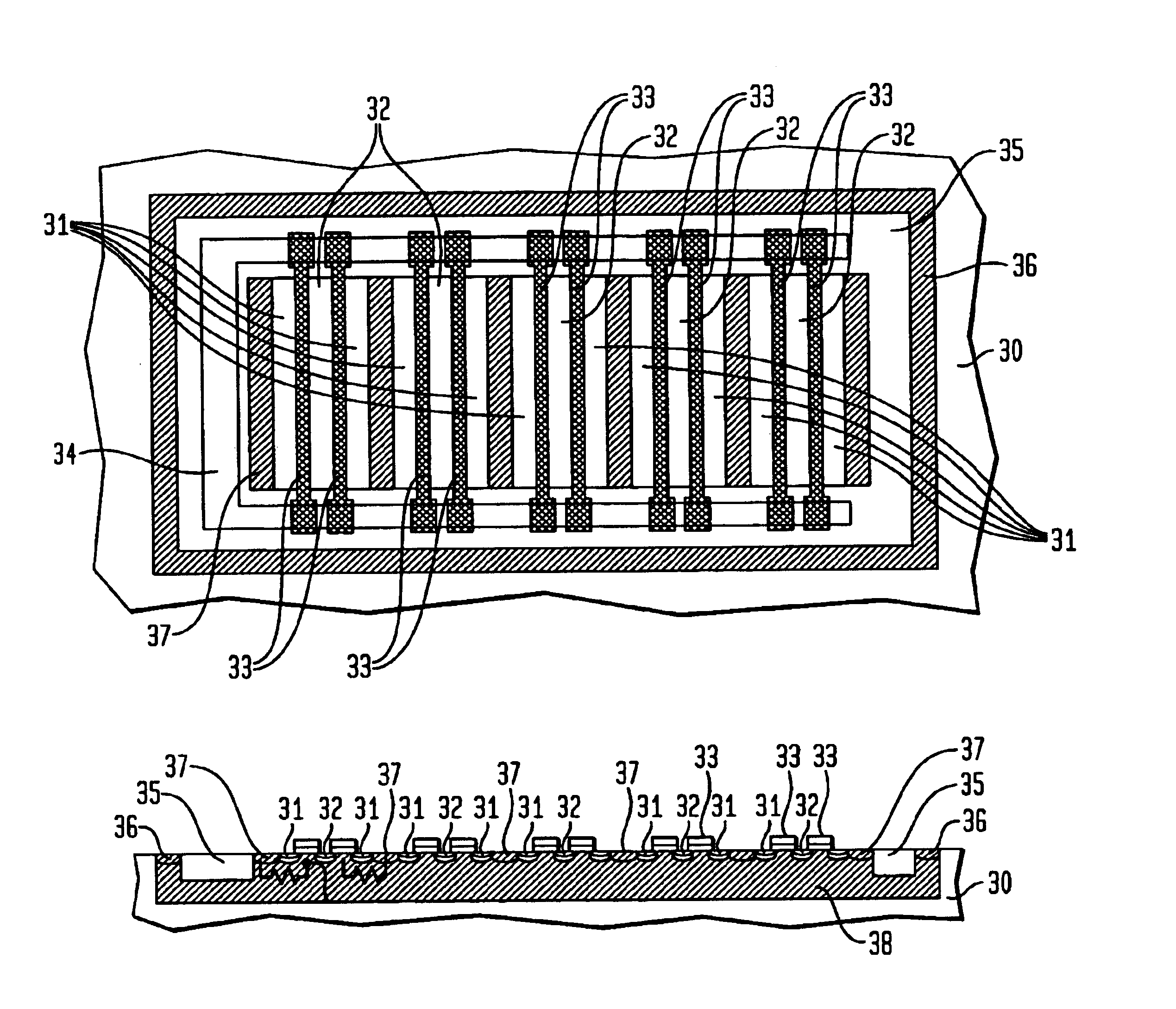
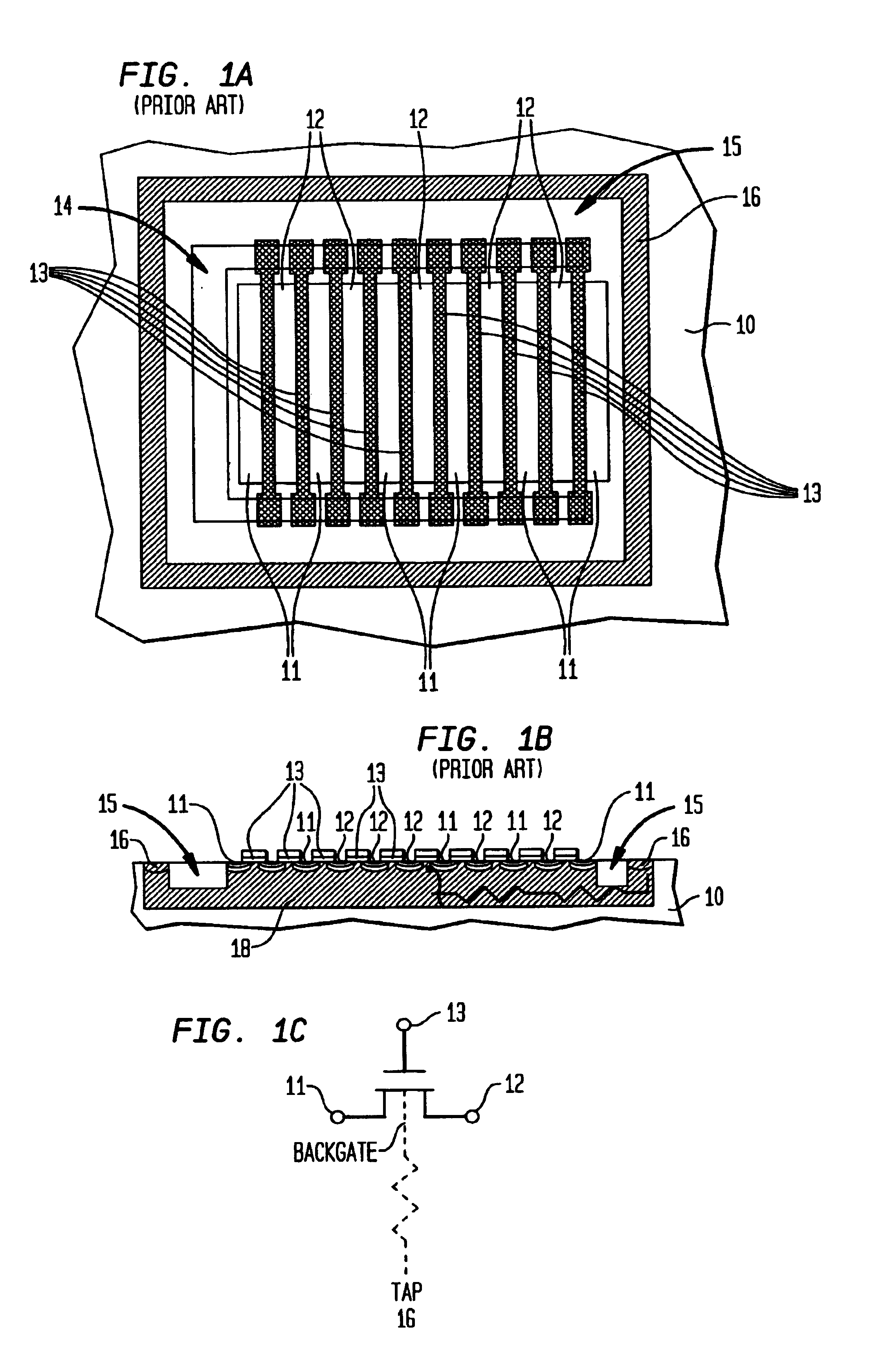
[0011]FIGS. 1A and 1B illustrate a conventional RF NMOS transistor in a semiconductor substrate 10. The transistor has a plurality of source regions 11 that are interdigitated with drain regions 12. The source and drain regions 11, 12 are formed by N+-type regions formed in a P-type well 18 in the substrate 10. Gate electrodes 13 lie over channel regions between the source and drain regions 11, 12 and are connected in parallel by a metal interconnect 14. The source and drain regions 11, 12 are likewise connected in parallel respectively. The interconnects for these parallel connections are not shown in the drawings. Isolating the source and gate regions 11, 12 is an insulating oxide layer 15 in a trench surrounding the regions 11, 12. A P+-type tap 16 rings the oxide layer 15 (and source and gate regions 11, 12) at the periphery of the transistor and provides an electrical contact to the P-well 18 in that the source and drain regions 11, 12 are located.

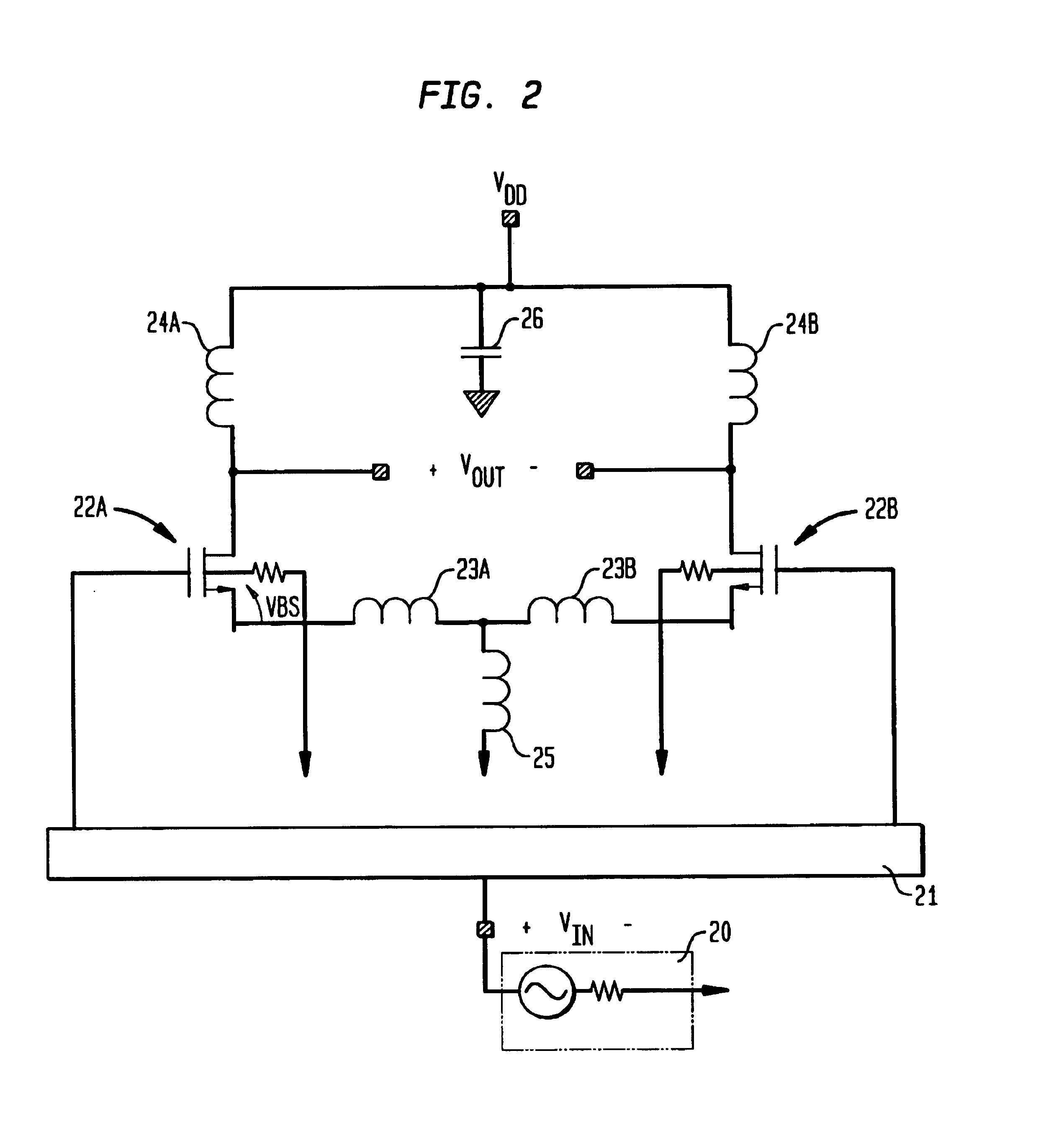
[0012]FIG. 1C is a circuit ele...


PUM


Abstract

An RF MOS transistor having improved AC output conductance and AC output capacitance includes parallel interdigitated source and drain regions separated by channel regions and overlying gates. Grounded tap regions contacting an underlying well are placed contiguous to source regions and reduce distributed backgate resistance, lower backgate channel modulation, and lower output conductance.

Description

BACKGROUND OF THE INVENTION[0001]The present invention is related to the design of MOS transistors and, in particular, to the design of MOS transistors operating in the RF frequency region.[0002]Current semiconductor processing technologies have enabled the reduction of sizes of transistors with critical dimensions below 0.25 μm. Critical dimensions are now approaching 0.18 μm and even more aggressive technologies are considering critical dimensions of 0.13 μm. The operating frequencies of the resulting integrated circuits have risen to such an extent that MOS (Metal-Oxide-Semiconductor) integrated circuits are being used for RF (Radio Frequency) applications.[0003]However, at high frequencies the transistors operate less efficiently in some applications. This is especially true when the MOS transistor is used in a receiving circuit, which is required to have high linearity and low-noise. The AC output conductance and the AC output capacitance of the transistor are adversely affecte...

Claims


Application Information

Patent Timeline
Patent Type & Authority Patents(United States)
IPC IPC(8): H01L29/76H01L29/06H01L29/10H01L29/417H01L29/78
CPCH01L29/0692H01L29/1087H01L29/78H01L29/41758
Inventor MCKAY, THOMAS G.ALLOTT, STEPHEN
Owner GATX VENTURES
Why Eureka
Try Eureka