CMOS device

a technology of mosfets and cmos, which is applied in the direction of mosfets, basic electric elements, electrical apparatus, etc., can solve the problems of complicated process of strained-si mosfets fabrication, and achieve the effect of improving the mobility of holes and electrons within the structur

Inactive Publication Date: 2006-04-04
TAIWAN SEMICON MFG CO LTD
View PDF15 Cites 90 Cited by
  • Summary
  • Abstract
  • Description
  • Claims
  • Application Information

AI Technical Summary

Benefits of technology

[0013]It has now been discovered that the above and other objects of the present invention may be accomplished in the following manner. Specifically, a structure having at least an adjacent NMOS device and PMOS device is provided. A first stress layer is formed over the PMOS device and a second stress layer is formed over the NMOS device whereby the mobility of holes and electrons within the struc

Problems solved by technology

However, the fabrication of strained-Si MOSFETs involves comp

Method used


Image

  • CMOS device
  • CMOS device
  • CMOS device

Examples


Embodiment Construction

Information Known to the Inventors—Not to be Considered Prior Art

[0016]The following information is known to the inventors and is not to be necessarily considered prior art for the purposes of this invention.

[0017]Changing the Si lattice spacing to a value other than the equilibrium value by using mechanical stress can increase the mobility of holes and electrons. This has been demonstrated in a strained-silicon (Si) MOSFET which applied high biaxial tensile stress to the channel of MOSFETs. However, the fabrication of strained-Si MOSFETs involves complicated processes such as forming a relaxed SiGe buffer layer. A recent study has shown that mechanical stress from a contact etch stop silicon nitride (SiN) layer affects the drive current.

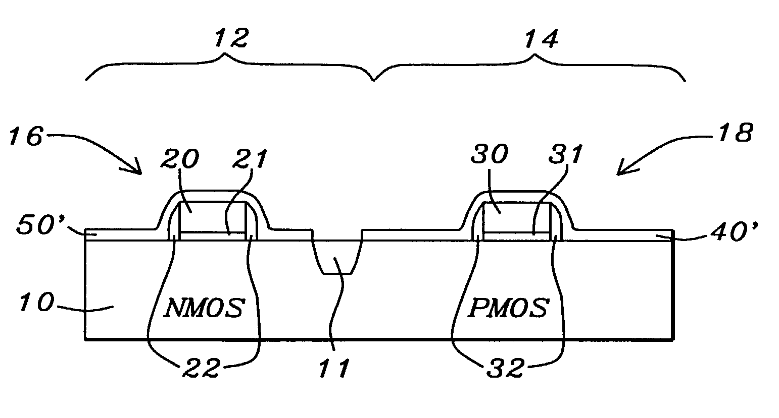
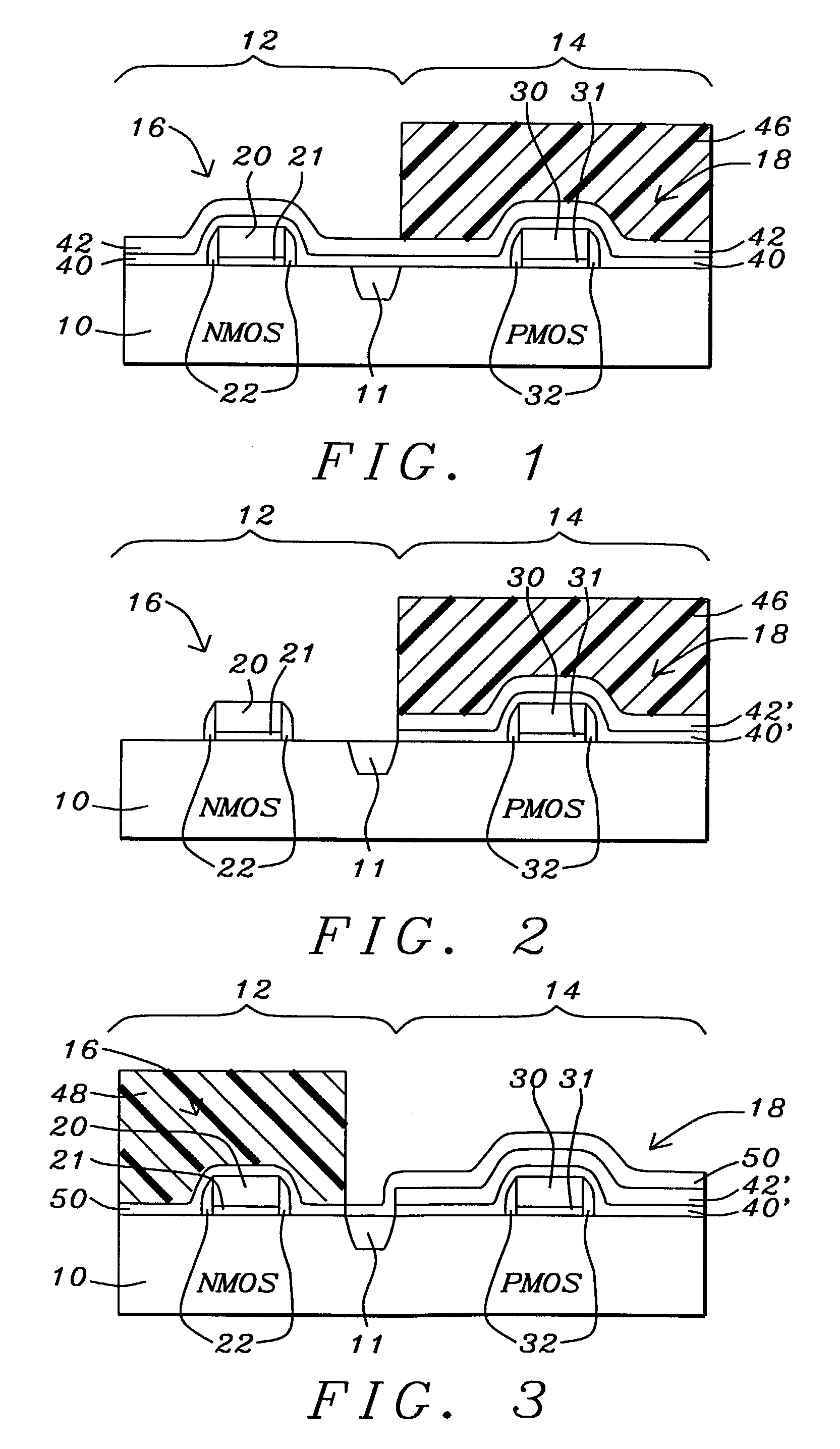
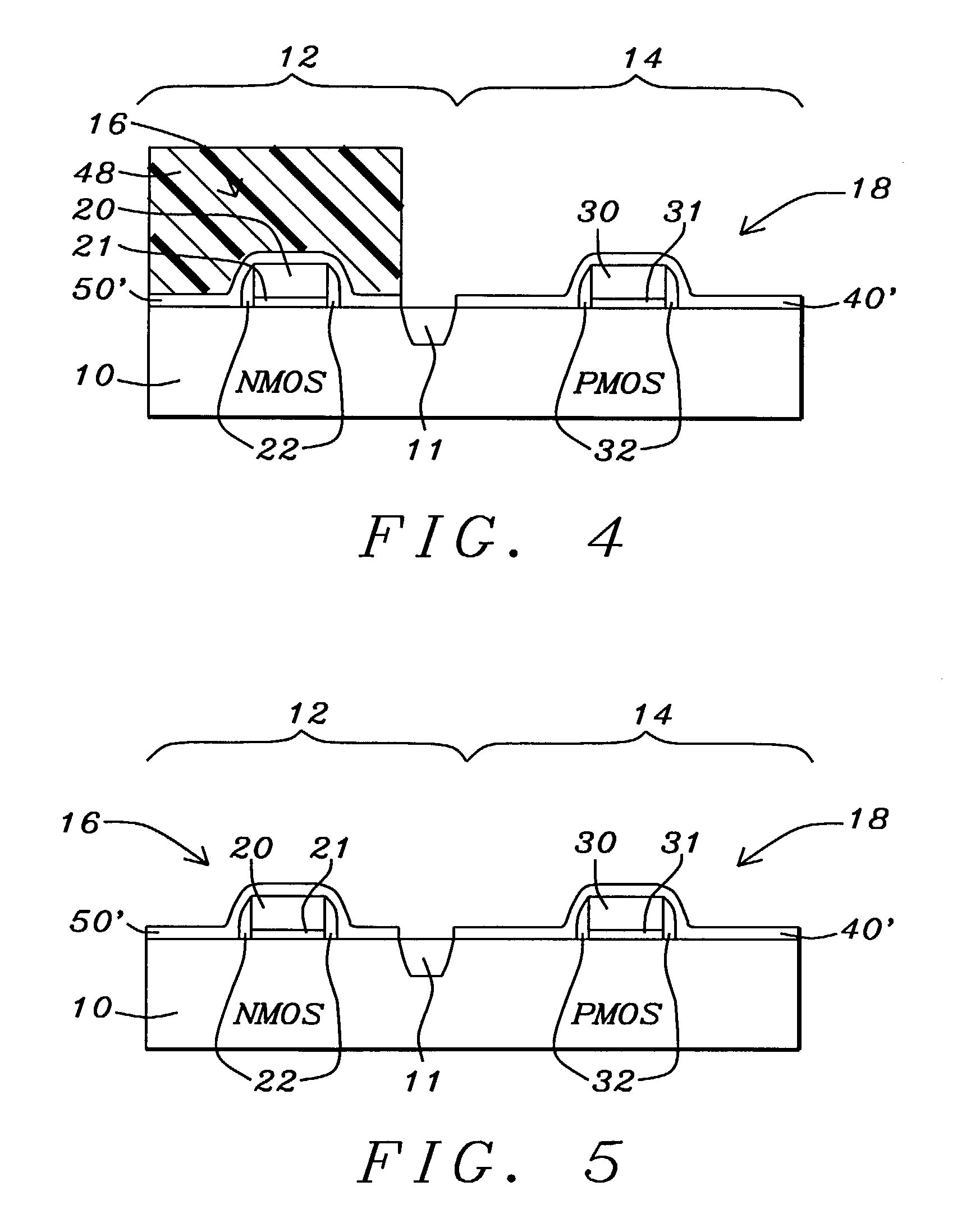
[0018]Initial Structure—FIG. 1 As shown in FIG. 1, the preferred structure of the present embodiment includes a structure 10 that preferably includes (1) at least one NMOS region 12 having at least one NMOS (N-type MOS) device 16 formed therein and ...


PUM


Abstract

A method comprising providing a substrate having an NMOS device adjacent a PMOS device and forming a first stress layer over the NMOS and PMOS devices, wherein the first stress layer comprises a first tensile-stress layer or a compression-stress layer. An etch stop layer is formed over the first stress layer, and portions of the first stress layer and the etch stop layer are removed from over the NMOS device, leaving the first stress layer and the etch stop layer over the PMOS device. A second tensile-stress layer is formed over the NMOS device and over the first stress layer and the etch stop layer, and portions of the second tensile-stress layer and the etch stop layer are removed from over the PMOS device, leaving the second tensile-stress layer over the NMOS device.

Description

BACKGROUND OF THE INVENTION[0001]Mechanical stress control in the channel regions of metal-oxide semiconductor field-effect transistors (MOSFETs) enables overcoming the limitations incurred in the scaling down of devices.[0002]U.S. Pat. No. 6,284,610 B1 to Cha et al. describes a poly layer to reduce stress.[0003]U.S. Pat. No. 6,281,532 B1 to Doyle et al. describes processes to change the localized stress.[0004]U.S. Pat. No. 5,562,770 to Chen et al. describes a process for global stress modification by forming layers or removing layers from over a substrate.[0005]U.S. Pat. No. 5,834,363 to Masanori describes a method for global stress modification by forming layers from over a substrate.[0006]The J. Welser et al. Strain Dependence of the Performance Enhancement in Strained-Si n-MOSFETs, IEDM Tech. Dig., pp. 373–376, 1994 article discloses measurements of the strain dependence of the electron mobility enhancements in n-MOSFETs employing tensilely-strained Si channels.[0007]The K. Rim ...

Claims


Application Information

Patent Timeline
IPC IPC(8): H01L21/336H01L21/8238
CPCH01L21/823807H01L29/7843H01L21/823828
Inventor HUANG, CHIEN-CHAOWANG, CHAO-HSINGGE, CHUNG-HUHU, CHENMING
Owner TAIWAN SEMICON MFG CO LTD
Why Eureka
Try Eureka