Dynamic burn-in equipment

a technology of burn-in acceleration and equipment, which is applied in the direction of individual semiconductor device testing, fault location by increasing destruction at fault, etc., can solve the problems of inability to analyze in detail, burn-in acceleration test is not always conducted at the expected temperature inside the chip, and burn-in acceleration test is not always conducted with a proper burn-in time, etc., to achieve accurate control of the temperature inside the chip

Inactive Publication Date: 2006-04-04
FUJITSU LTD
View PDF11 Cites 69 Cited by
  • Summary
  • Abstract
  • Description
  • Claims
  • Application Information

AI Technical Summary

Benefits of technology

[0013]The present invention has been developed in order to solve the above-mentioned problems of the prior art and the object thereof is to provide a burn-in equipment

Problems solved by technology

However, in a conventional burn-in equipment, the power source current may fluctuate because of the variations in the quality of production lots the semiconductor devices, therefore, the burn-in acceleration test was not always conducted at an expected temperature i

Method used


Image

  • Dynamic burn-in equipment
  • Dynamic burn-in equipment
  • Dynamic burn-in equipment

Examples


first embodiment

[0051](1) First Embodiment

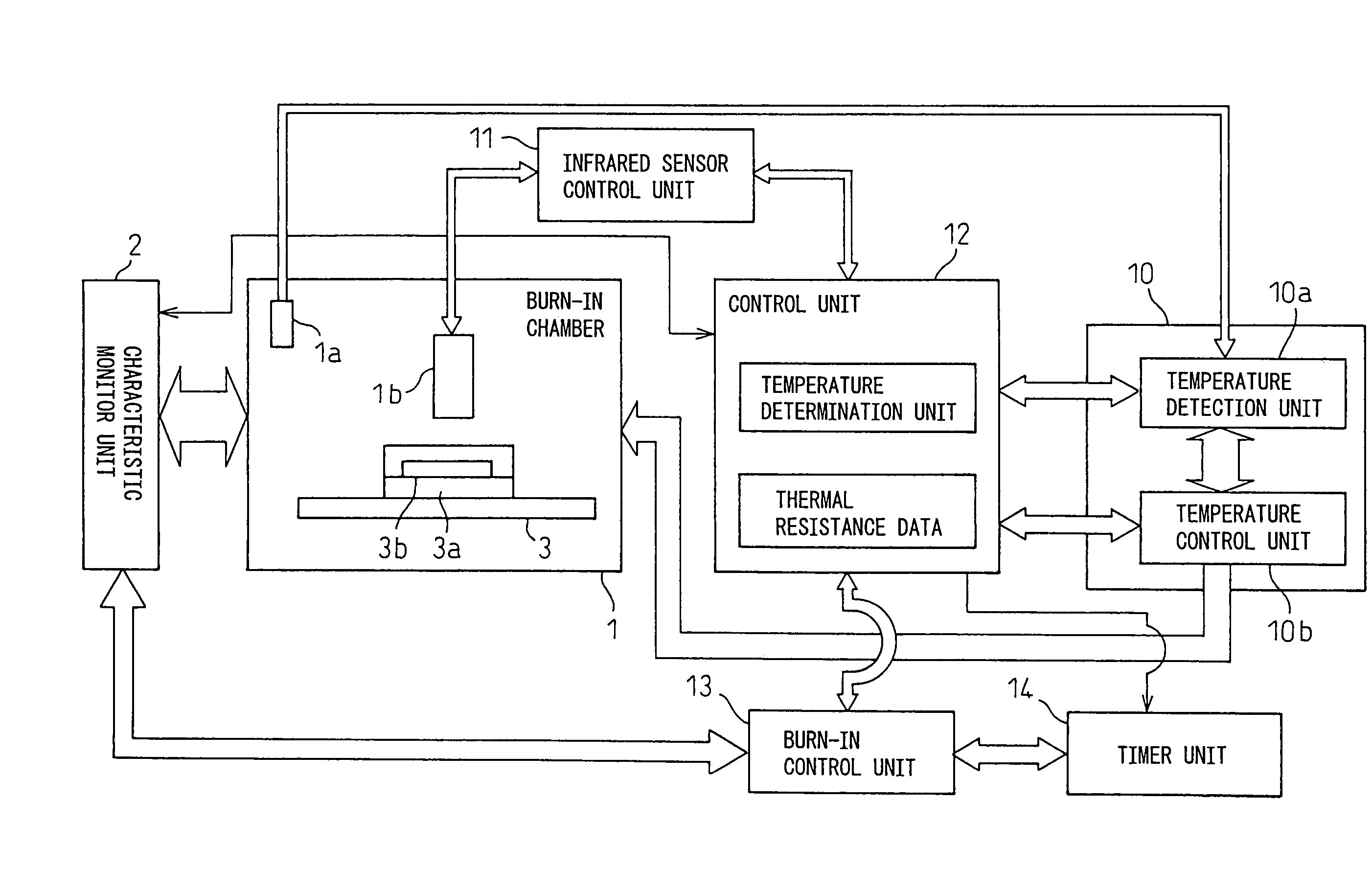
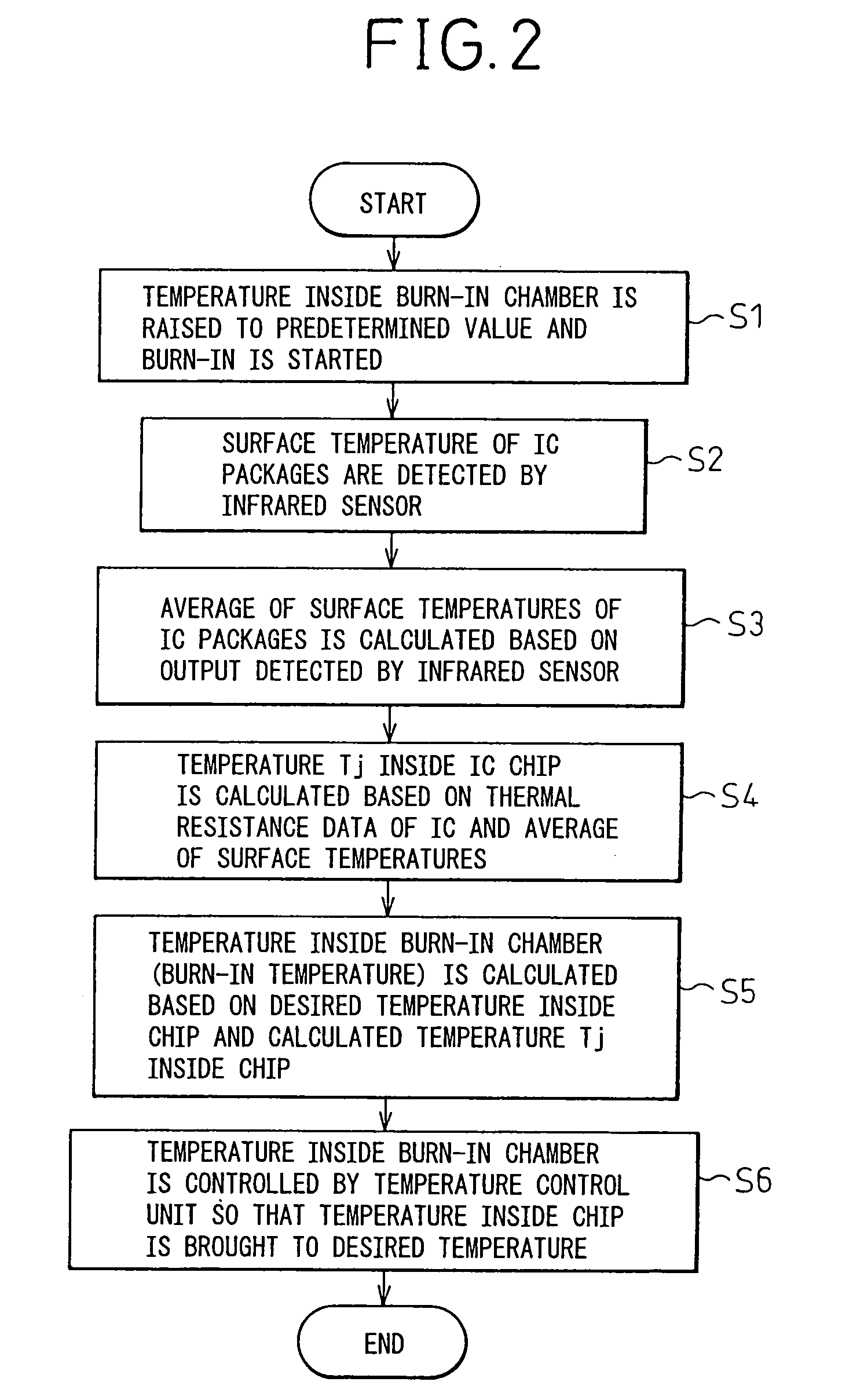
[0052]Conventionally, as described above, a burn-in acceleration test is not always conducted at an expected temperature Tj inside a chip because of the variations in the quality of ICs. In the present embodiment, therefore, the temperature inside an IC chip is found based on the surface temperature of the IC mounted on a burn-in card accommodated in a burn-in chamber and the temperature inside the burn-in chamber is set to an optimum value.

[0053]FIG. 2 is a flow chart showing a series of processes performed by the control unit 12 in the present embodiment and the present embodiment is explained with reference to FIG. 2.

[0054]A burn-in card on which an IC has been mounted is accommodated in the burn-in chamber 1 as shown in FIG. 1. The control unit 12 raises the temperature inside the burn-in chamber 1 to a predetermined temperature by using the temperature controller 10 and sends out a burn-in start signal to the burn-in control unit 13 (step S1 in FIG. 2)...

second embodiment

[0061](2) Second Embodiment

[0062]As described above, when a life test or the like of semiconductor devices is conducted, the burn-in time is determined based on the acceleration coefficient (product of the temperature inside the chip and the voltage) and the acceleration period given in advance.

[0063]According to the first embodiment described above, as the temperature inside the chip can be brought to a desired value, it is possible to accurately obtain the acceleration coefficient. Therefore, in the second embodiment, the burn-in time is calculated based on the obtained acceleration coefficient as above mentioned and the acceleration period given in advance. The burn-in is conducted with the calculated burn-in time, and the life test of the semiconductor devices are conducted.

[0064]FIG. 3 is a flow chart showing a series of processes performed by the control unit 12 and the second embodiment will be explained with reference to FIG. 3.

[0065]A burn-in card on which an ICs have been ...

third embodiment

[0073](3) Third Embodiment

[0074]In order to conduct a particular analysis or the like of a defective IC, the IC can be examined to specify a defective portion. In the third embodiment, when a defective IC is found during the burn-in acceleration test, it is possible to efficiently carry out the analysis of the defective IC by specifying the defective portion of the defective IC based on the surface temperature distribution of the defective IC.

[0075]FIG. 4 is a flow chart showing a series of processes performed by the control unit 12 in the third embodiment and the embodiment will be explained with reference to FIG. 4.

[0076]As described in the first and second embodiments, a burn-in card on which an IC has been mounted is accommodated in the burn-in chamber 1, a temperature inside the burn-in chamber 1 is raised to a predetermined temperature, a burn-in signal is sent out to each IC 3b mounted on the burn-in card 3 in the burn-in chamber 1 from the characteristic monitoring unit 2, a...


PUM


Abstract

An infrared sensor is provided in a burn-in chamber. The surface temperatures of two or more semiconductor devices are measured by the sensor. A control unit calculates the internal temperatures of the semiconductor devices based on the thermal resistance values of the semiconductor device packages and controls the temperature inside the burn-in chamber so that the average of the internal temperatures is brought to a desired temperature by using a temperature controller. Further, an acceleration coefficient is obtained based on the internal temperatures, a burn-in time is determined based on the acceleration coefficient and a preliminarily given accelerated period, and a burn-in acceleration test is conducted. Moreover, when a defective semiconductor is found, the defective portion of the defective semiconductor device is specified based on the surface temperature distribution of the semiconductor device measured by the infrared sensor.

Description

CROSS-REFERENCE TO RELATED APPLICATIONS[0001]This application is based upon, and claims the priority of, Japanese Patent Application No. 2001-386153, filed on Dec. 19, 2001, the contents being incorporated herein by reference, and a continuation of PCT / JP02 / 12854, filed on Dec. 9, 2002.BACKGROUND OF THE INVENTION[0002]1. Field of the Invention[0003]The present invention relates to a burn-in equipment for screening out a defective semiconductor and, more particularly, to a burn-in equipment capable of conducting burn-in at an optimally set burn-in temperature.[0004]2. Description of the Related Art[0005]Conventionally, dynamic burn-in screen test is carried out when, for example, semiconductor devices are received, by burning in the semiconductor devices in a burn-in chamber while inputting burn-in signals to the semiconductor devices from a signal generator.[0006]A burn-in equipment comprises, for example, a burn-in chamber, a characteristic monitoring unit made up of an IC tester, ...

Claims


Application Information

Patent Timeline
IPC IPC(8): G01R31/302G01R31/26G01R31/28G01R31/30
CPCG01R31/2874G01R31/2862
Inventor MAESAKI, YOSHIHIROTESHIGAWARA, HIROSHI
Owner FUJITSU LTD
Why Eureka
Try Eureka