Development apparatus for manufacturing semiconductor device

a technology for semiconductor devices and development apparatuses, applied in photomechanical apparatus, instruments, photosensitive materials, etc., can solve the problems of wasting a considerable amount of developer and reducing the uniformity of resist patterns, and achieve the effect of efficient application of developer

Inactive Publication Date: 2006-04-11
LAPIS SEMICON CO LTD
View PDF2 Cites 4 Cited by
  • Summary
  • Abstract
  • Description
  • Claims
  • Application Information

AI Technical Summary

Benefits of technology

[0010]Accordingly, it is an object of the present invention to provide a development apparatus capable of efficient...

Problems solved by technology

It, however, causes a great impact on the surface of the substrate 5, which results in decrease of the uniformity of the resist patt...

Method used


Image

  • Development apparatus for manufacturing semiconductor device
  • Development apparatus for manufacturing semiconductor device
  • Development apparatus for manufacturing semiconductor device

Examples


first embodiment

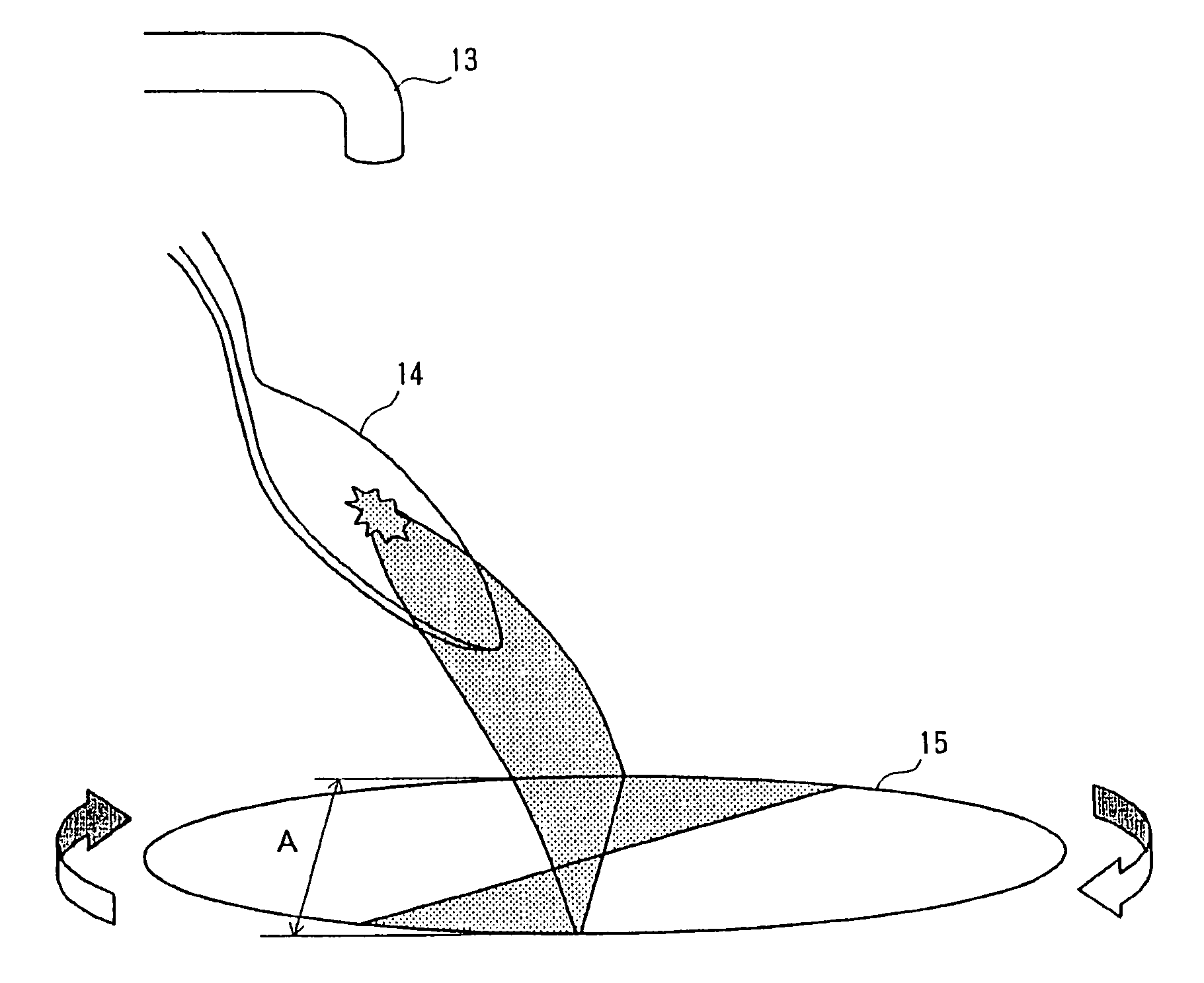
[0027]As described above, it is possible to provide a widely spread coating at a constant pressure without changing the discharge pressure and the nozzle.

second embodiment

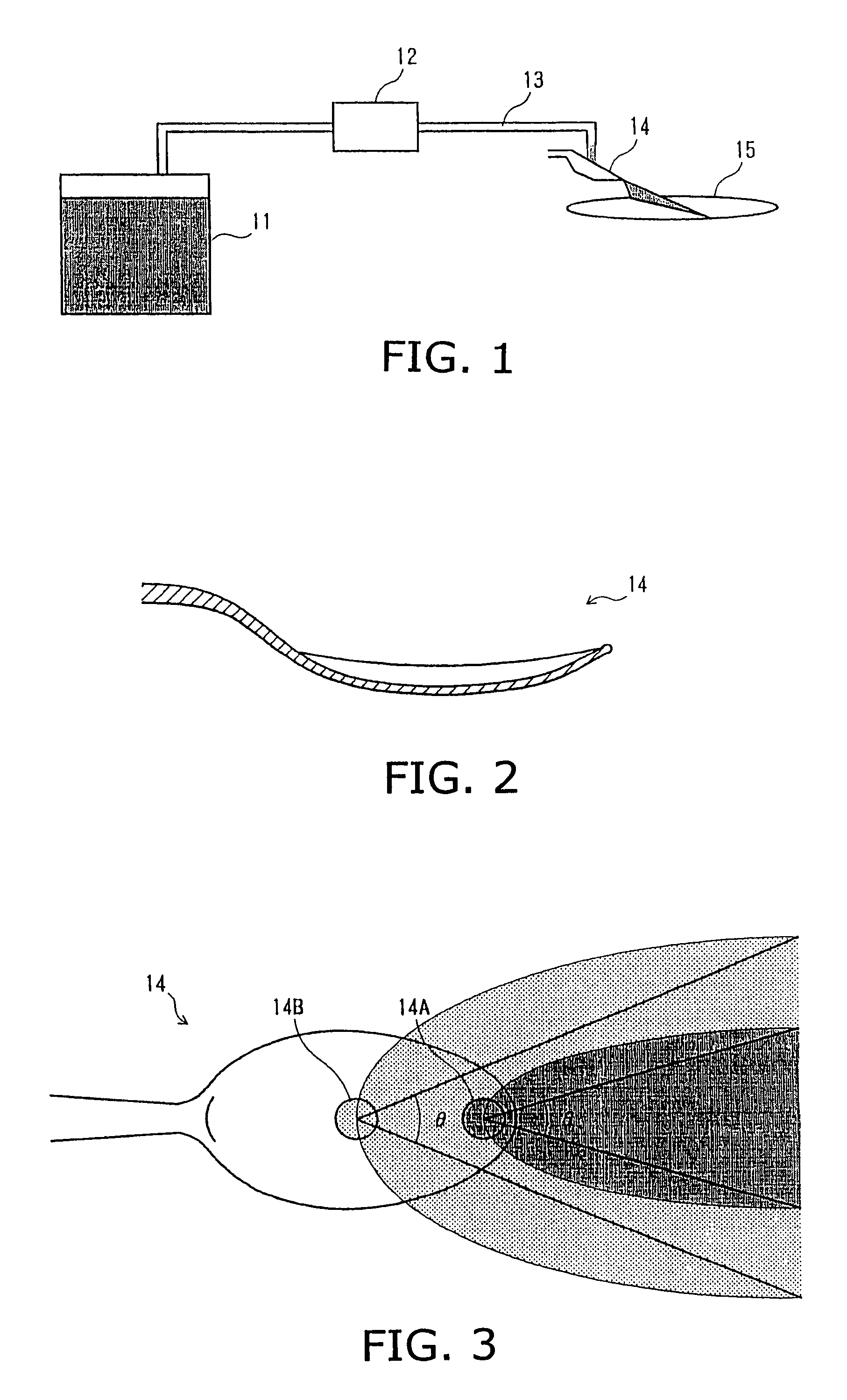
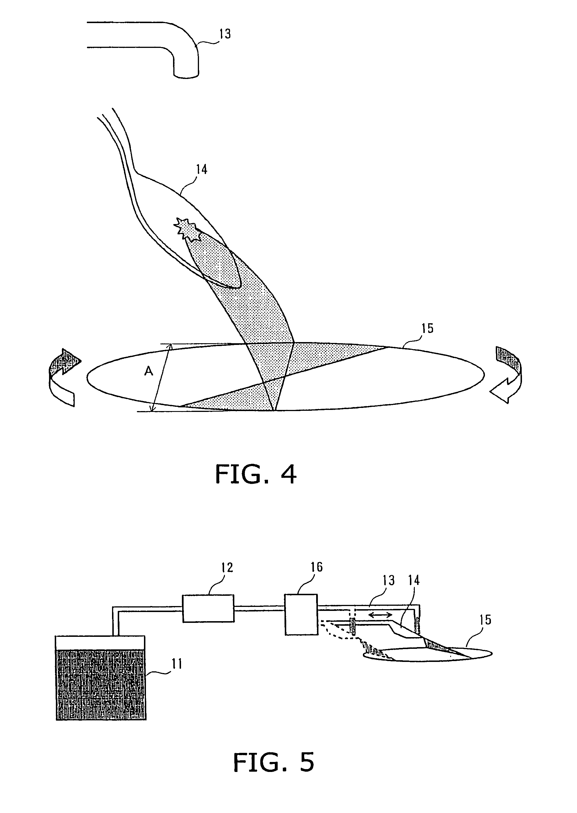
[0028]In FIG. 5, reference numeral 16 denotes a nozzle adjustment mechanism. In the second embodiment, the positions of the nozzle pipe and the nozzle are adjusted by the nozzle adjustment mechanism 16 with the substrate fixed without any rotation.

[0029]In FIG. 6, reference number 15A denotes a first position (right-hand position) of the substrate 15, 15B a second position (quarter position) of the substrate 15, 15C a third position (half position) of, 15D a fourth position (three-quarter position), and 15E a fifth position (left-hand position). That is, the nozzle 14 is slid from a position {circle around (1)} to a position {circle around (5)} for coating the substrate 15. At this point, the developer discharge position to the nozzle 14 is adjusted by sliding the nozzle pipe 13 such that the width A of the sprayed developer becomes equal to the width of each sprayed position of the substrate 15.

[0030]For example, when the substrate 15 is coated from the first position 15A to the th...


PUM


Abstract

A development apparatus for discharging a developer onto a surface of a semiconductor substrate (15) comprises a nozzle pipe (13) for supplying the developer, and a nozzle (14) having a shape of a spoon with a taper and discharging the developer supplied by the nozzle pipe onto the surface of the substrate. The nozzle sprays the developer onto the surface of the substrate at any spray angle under a low and constant pressure.

Description

BACKGROUND OF THE INVENTION[0001]1. Field of the Invention[0002]The present invention relates to a development apparatus useful for manufacturing a semiconductor device, especially to a discharge nozzle useful for the development process.[0003]2. Description of the Related Art[0004]FIG. 9 is a schematic diagram of a conventional development apparatus used in manufacturing a semiconductor.[0005]The conventional development apparatus comprises a developer tank 1, an electromagnetic valve 2, a nozzle pipe 3, and a spray nozzle (nozzle tip) 4. The surface of a substrate 5 is coated with a developer sprayed by the spray nozzle 4. The substrate 5 is left for tens of seconds with the coated developer so that a photo-resist film is reacted with the developer to create a pattern.[0006]The coating of the surface of the substrate 5 with the developer by the spray nozzle 4 is performed such that the developer is discharged in a shape of fan in order to coat a large area of the substrate 5 in a ...

Claims


Application Information

Patent Timeline
IPC IPC(8): G03D5/04G03F7/30H01L21/00H01L21/027
CPCH01L21/6715G03F7/3021
Inventor SHIMADA, KEIZOOHTA, YASUHARU
Owner LAPIS SEMICON CO LTD
Why Eureka
Try Eureka