Method for cleaning semiconductor wafers

a technology for cleaning and semiconductor wafers, applied in the direction of detergent compounding agents, cleaning using liquids, physical/chemical process catalysts, etc., can solve the problems of complex and inconvenient implementation, and achieve the effect of low cost and high efficiency

Inactive Publication Date: 2006-04-18
HON HAI PRECISION IND CO LTD
View PDF6 Cites 23 Cited by
  • Summary
  • Abstract
  • Description
  • Claims
  • Application Information

AI Technical Summary

Benefits of technology

[0007]In view of the above-described shortcomings, an object of the present invention is to provide a simple, low cost and highly efficient method for cleaning a surface of a semiconductor wafer.

Problems solved by technology

The method includes at least four steps, and is complex and inconvenient to implement.
It is also expensive since a multitude of devices and chemical reagents must be used.

Method used


Image

  • Method for cleaning semiconductor wafers
  • Method for cleaning semiconductor wafers

Examples


Embodiment Construction

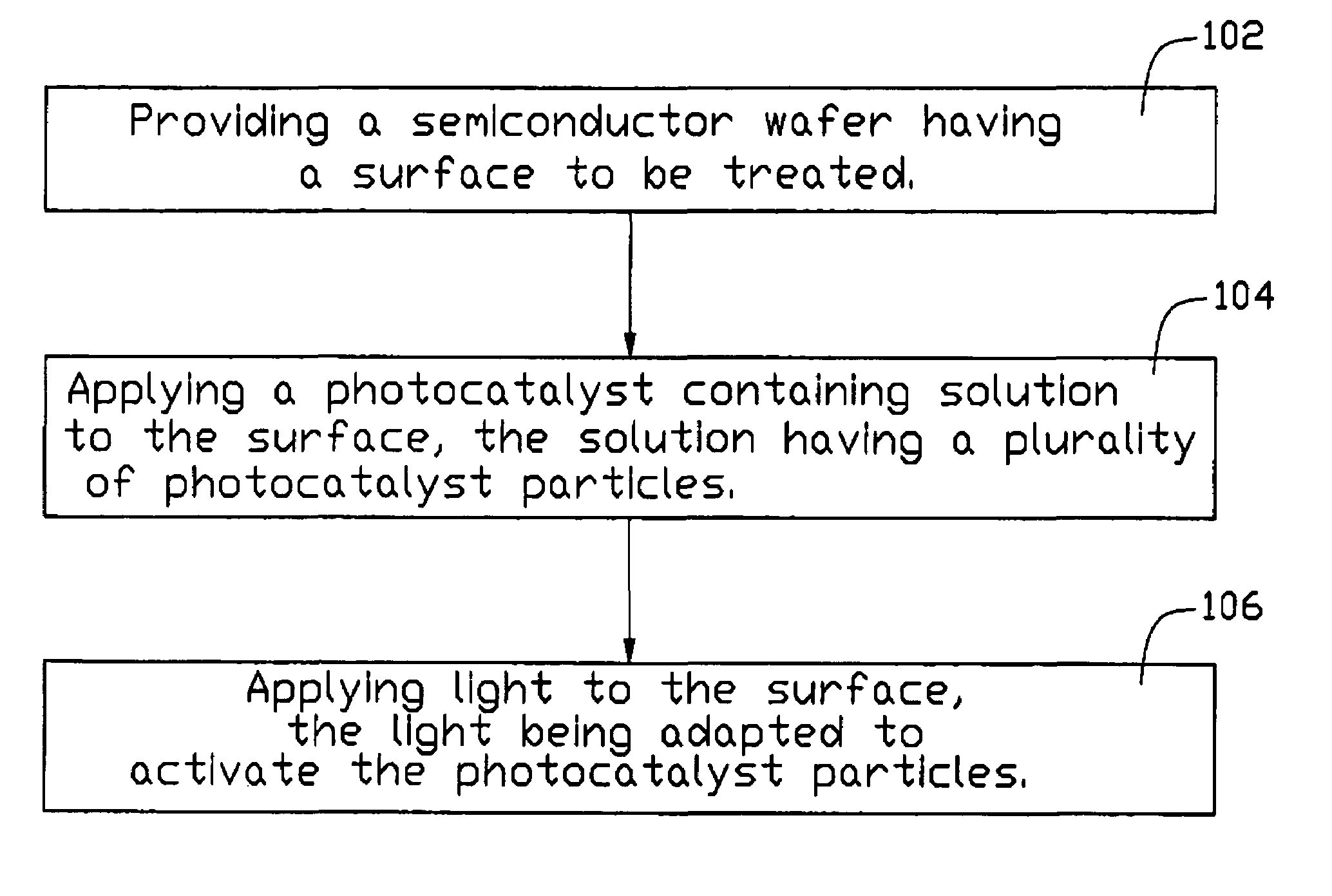
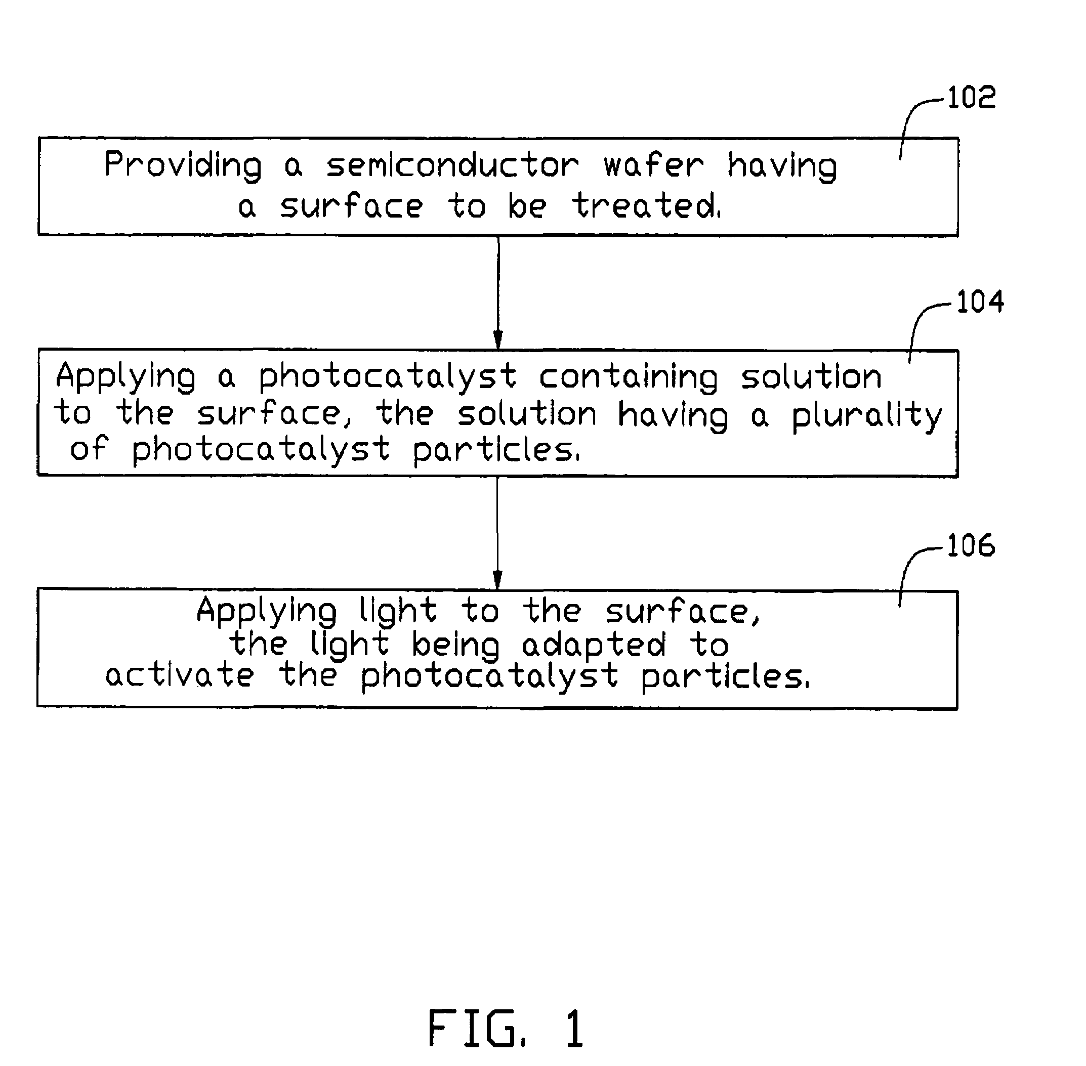
[0011]Reference will now be made to the drawings to describe the preferred method of the present invention in detail.

[0012]Referring to FIG. 1, a method for cleaning a surface of semiconductor wafer after chemical mechanical polishing in accordance with the preferred embodiment of the present invention comprises the steps of: (1) providing a semiconductor wafer having a surface to be treated; (2) applying a photocatalyst containing solution to the surface, the solution having a plurality of photocatalyst particles; and (3) applying light to the surface, the light being adapted to activate the photocatalyst particles.

[0013]In step (1), generally designated with 102, a semiconductor wafer having a surface to be treated is provided. The surface has already undergone CMP. After the CMP, contaminants remain on the surface. These contaminants may, for example, include slurry particle remnants, metal ion remnants and organic compound remnants. The contaminants generally have an adverse eff...


PUM

PropertyMeasurementUnit
diametersaaaaaaaaaa
wavelengthaaaaaaaaaa
sizesaaaaaaaaaa

Abstract

A method for cleaning a surface of semiconductor wafer after chemical mechanical polishing in accordance with the present invention comprises the steps of: (1) providing a semiconductor wafer having a surface to be treated; (2) applying a photocatalyst containing solution to the surface, the solution having a plurality of photocatalyst particles; and (3) applying light to the surface, the light being adapted to activate the photocatalyst particles.

Description

BACKGROUND OF THE INVENTION[0001]1. Field of the Invention[0002]The present invention relates to a method for processing a semiconductor wafer, and more particularly to a method for cleaning a surface of a semiconductor wafer after chemical mechanical polishing.[0003]2. Description of Related Art[0004]In the semiconductor processing industry, chemical mechanical polishing (CMP) is known as one of the best techniques for planarizing and polishing a surface of a semiconductor wafer. CMP generally involves a polishing slurry composition which often contains abrasive particles such as silica and alumina in an acidic or basic solution. Typically, an aqueous solution is used to remove the particles and contaminants away from the surface after the CMP is completed. For instance, U.S. Pat. No. 6,537,381 discloses a method for cleaning and treating a semiconductor wafer after CMP. An improved cleaning chemical (ICC) is applied in the method. The ICC solution preferably includes ammonium hydr...

Claims


Application Information

Patent Timeline
Patent Type & Authority Patents(United States)
IPC IPC(8): B24B1/00B08B7/00C11D11/00H01L21/306
CPCB08B7/0035C11D3/0063H01L21/02052C11D11/0047C11D3/1213
Inventor CHEN, GA-LANE
Owner HON HAI PRECISION IND CO LTD
Why Eureka
Try Eureka