Integral polishing pad and manufacturing method thereof

a polishing pad and integrated technology, applied in the field of polishing pads, can solve the problems of reducing the planarization efficiency, affecting the manufacturing process, and affecting the quality of the polishing pad, and achieve the effect of improving the planarization efficiency

Inactive Publication Date: 2006-04-18
KPX CHEM
View PDF6 Cites 54 Cited by
  • Summary
  • Abstract
  • Description
  • Claims
  • Application Information

AI Technical Summary

Benefits of technology

[0007]The present invention provides an integral polishing pad with improved planarization efficiency.
[0008]The present invention also provides an integral polishing pad, which allows the flatness of a wafer to be optically detected in situ and can be easily manufactured.
[0014]An integral polishing pad according to the present invention has high planarization efficiency and uniform properties, and thus can be reliably used for polishing. In addition, the present invention prevents a congestion of a polishing slurry, thereby preventing damage to a wafer, and facilitates delivery of the polishing slurry. Since the present invention provides an integral polishing pad, an adhesive for connecting elements or a process for bonding the elements is not required, so manufacturing processes are simplified.

Problems solved by technology

However, the resilient base layer cannot effectively act when the adhesive is nonuniformly applied, and therefore, the planarization efficiency is decreased.
In addition, applying the adhesive for connection of the two layers when manufacturing the polishing pad complicates manufacturing processes.
However, for the polishing pad disclosed in U.S. Pat. No. 5,605,760, it is necessary to punch a pad and attach a window transparent to a light beam, so manufacturing processes are complex.
In addition, a gap at a connection between the transparent window and the pad hinders the delivery of a polishing slurry, and a lump of the polishing slurry collected at the gap may scratch the surface of a wafer.
Since the material of the transparent window is different from that of the pad, a crack may occur around the transparent window during a polishing operation.
However, in order to manufacture this polishing pad, a special mold in which temperature can be differently adjusted depending on portions is required, and therefore, manufacturing cost is increased.
Moreover, since hysteresis loss cannot be minimized only by using a pad disclosed in U.S. Pat. No. 5,605,760 or 6,171,181, an elastic support layer is also required.
Here, it is necessary to form a transparent window or a transparent region in the elastic support layer, so manufacturing processes become complex.

Method used


Image

  • Integral polishing pad and manufacturing method thereof
  • Integral polishing pad and manufacturing method thereof
  • Integral polishing pad and manufacturing method thereof

Examples


experimental example 1

[0062]A reaction was commenced by mixing 100 g of a polyether-based isocyanate prepolymer (having an NCO content of 16%) with 100 g of polypropylene glycol at room temperature. Under the condition that a low viscosity is maintained, the mixed liquid was poured into a mold maintained at 80±1° C. Then, the resulting product was taken out and post cured for 20 hours in an oven maintained at 100° C. The cure product was cut to have a predetermined size, thereby forming a support layer. A sheet having a thickness of 1 mm was manufactured in the same manner as the support layer and cut to have a size of 20×50 mm, thereby manufacturing a transparent window.

[0063]The manufactured support layer was laid in a mold having a predetermined size, the transparent window was put on the surface of the support layer, and the temperature of the mold was set to 50° C.

[0064]100 g of a polyether-based isocyanate prepolymer (having an NCO content of 11%), 23.3 g of mineral oil (hereinafter, referred to as...

experimental example 2

[0065]An integral polishing pad was manufactured in the same manner as used in Experimental Example 1, with the exception that 46 g of KF-70 was used and EXPANCEL was not used.

experimental example 3

[0066]A polishing layer was manufactured in the same manner as used in Experimental Example 1. A predetermined portion of the polishing layer was punched in a size of 20×50 mm to form an empty space and then laid in a mold having a predetermined size. The temperature of the mold was set to 50° C.

[0067]A urethane reaction material manufactured by the same method as the transparent window was manufactured in Experimental Example 1 was injected into the empty space in the polishing layer within the mold. Thereafter, as in Experimental Example 1, a urethane reaction material for a support layer was injected into the mold. Next, gelling was performed for 30 minutes, and thereafter, curing was performed for 20 hours at 100° C. in an oven. The cured product was taken out of the mold and cut, thereby forming an integral polishing pad.

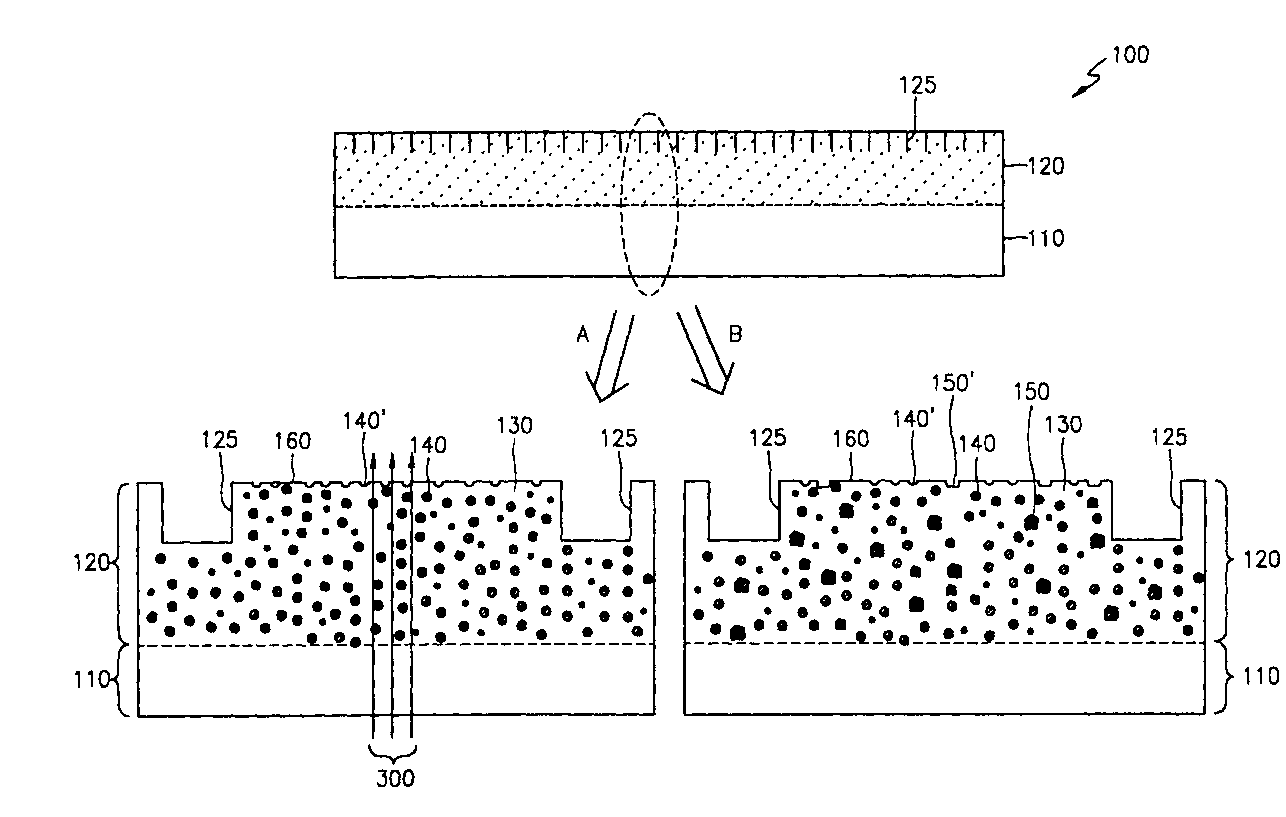
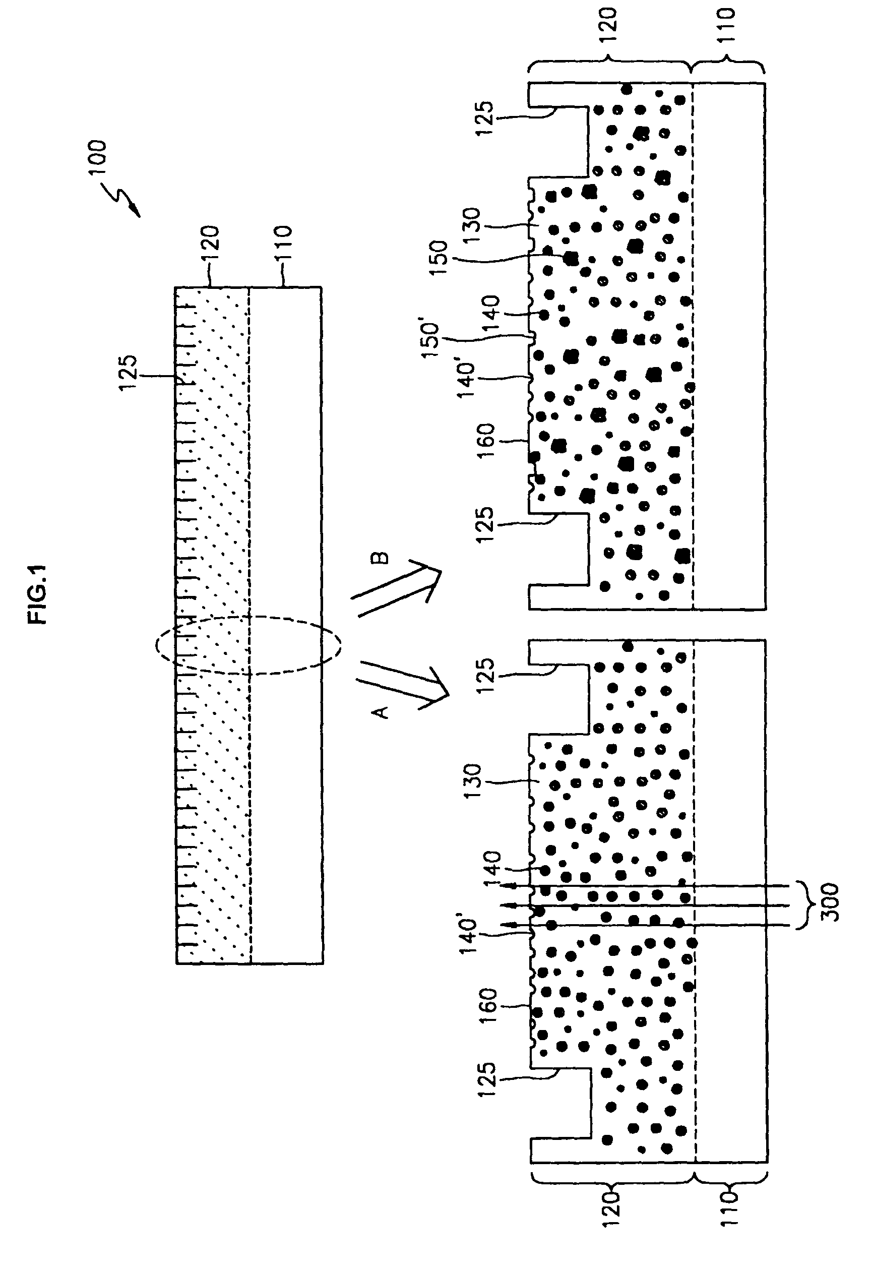
[0068]In an integral polishing pad according to the present invention, since an elastic support layer is integrated with a polishing layer, planarization effic...


PUM

PropertyMeasurementUnit
weight percentaaaaaaaaaa
diameteraaaaaaaaaa
diameteraaaaaaaaaa

Abstract

An integral polishing pad includes an elastic support layer and a polishing layer, which is formed on the elastic support layer and has a higher hardness than the elastic support layer. The elastic support layer and the polishing layer are made from materials chemically compatible with each other so that a structural border between the elastic support layer and the polishing layer does not exist. In addition, the integral polishing pad also includes a transparent region, which is transparent to a light source used to detect the surface state of an object being polished and integrated with the other elements of the integral polishing pad. The integral polishing pad has high planarization efficiency and uniform properties, and thus can be reliably used for polishing. In addition, the integral polishing pad prevents a congestion of a polishing slurry and facilitates delivery of the polishing slurry. The integral polishing pad does not need an adhesive for connecting elements or a process for bonding the elements, thereby simplifying manufacturing processes.

Description

BACKGROUND OF THE INVENTION[0001]1. Field of the Invention[0002]The present invention relates to a polishing pad and a manufacturing method thereof, and more particularly, to an integral polishing pad in which an elastic support layer and a polishing layer are integrated, and a manufacturing method thereof.[0003]2. Description of the Related Art[0004]Polishing speed and planarization performance are important in chemical mechanical polishing which is introduced for global planarization with the development of highly integrated and microscopic semiconductor devices and multilayer wiring structures. These are determined depending on the conditions of polishing equipment, the type of polishing slurry, the type of polishing pad, and the like. In particular, a polishing pad, which is in direct contact with a wafer during polishing and is an expendable element, is an important factor determining the polishing performance.[0005]In U.S. Pat. No. 5,257,478, an improved polishing pad, which m...

Claims


Application Information

Patent Timeline
Patent Type & Authority Patents(United States)
IPC IPC(8): B32B3/26B24B1/00B24D11/00B32B7/02C09K3/14B24B37/07B24B37/20B24B37/22B24B37/24B24D3/00B24D3/32H01L21/304
CPCB24B37/205B24D3/32Y10T428/24405Y10T428/24372Y10T428/24983Y10T428/2984Y10T428/24612Y10T428/249978Y10T428/24998Y10T428/249988B24D11/00
Inventor HUH, HYUNLEE, SANG-MOKSONG, KEE-CHEONKIM, SEUNG-GEUNSON, DO-KWON
Owner KPX CHEM
Why Eureka
Try Eureka