
Polishing slurries for copper and associated materials

a technology of polishing slurry and copper, which is applied in the direction of pigmentation treatment, electrical equipment, chemistry apparatus and processes, etc., can solve the problems of significant dishing of copper on the surface of the semiconductor wafer, poor removal of the barrier material, and unwanted dishing of copper and/or erosion of the dielectric material, etc., to achieve high removal rate, low removal rate, and high removal rate

Inactive Publication Date: 2006-04-20
CABOT MICROELECTRONICS CORP
View PDF14 Cites 2 Cited by
  • Summary
  • Abstract
  • Description
  • Claims
  • Application Information

AI Technical Summary

Benefits of technology

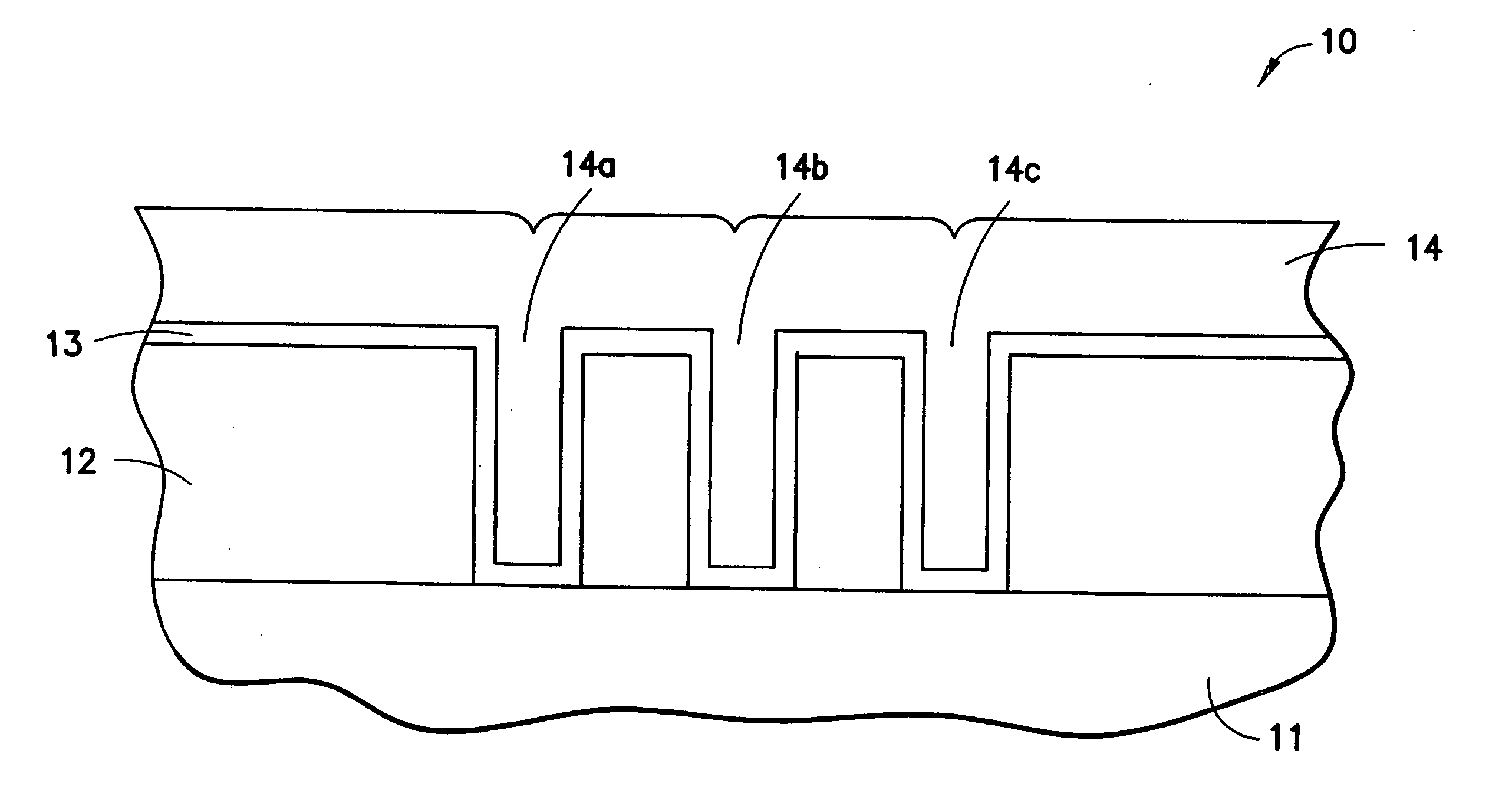
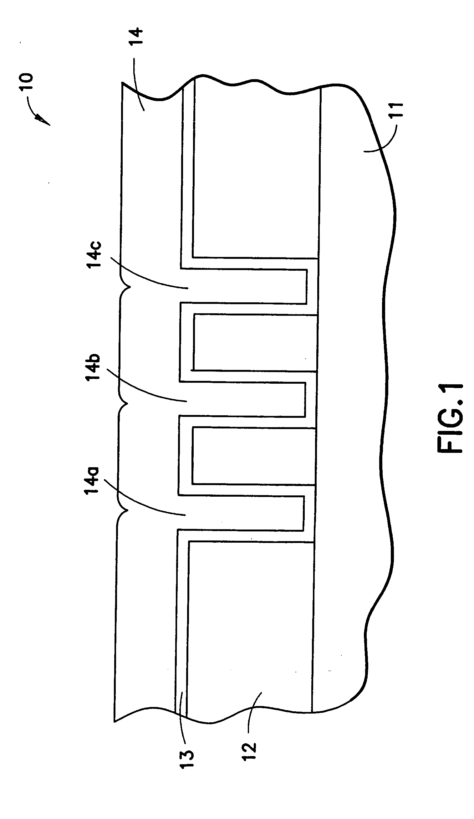
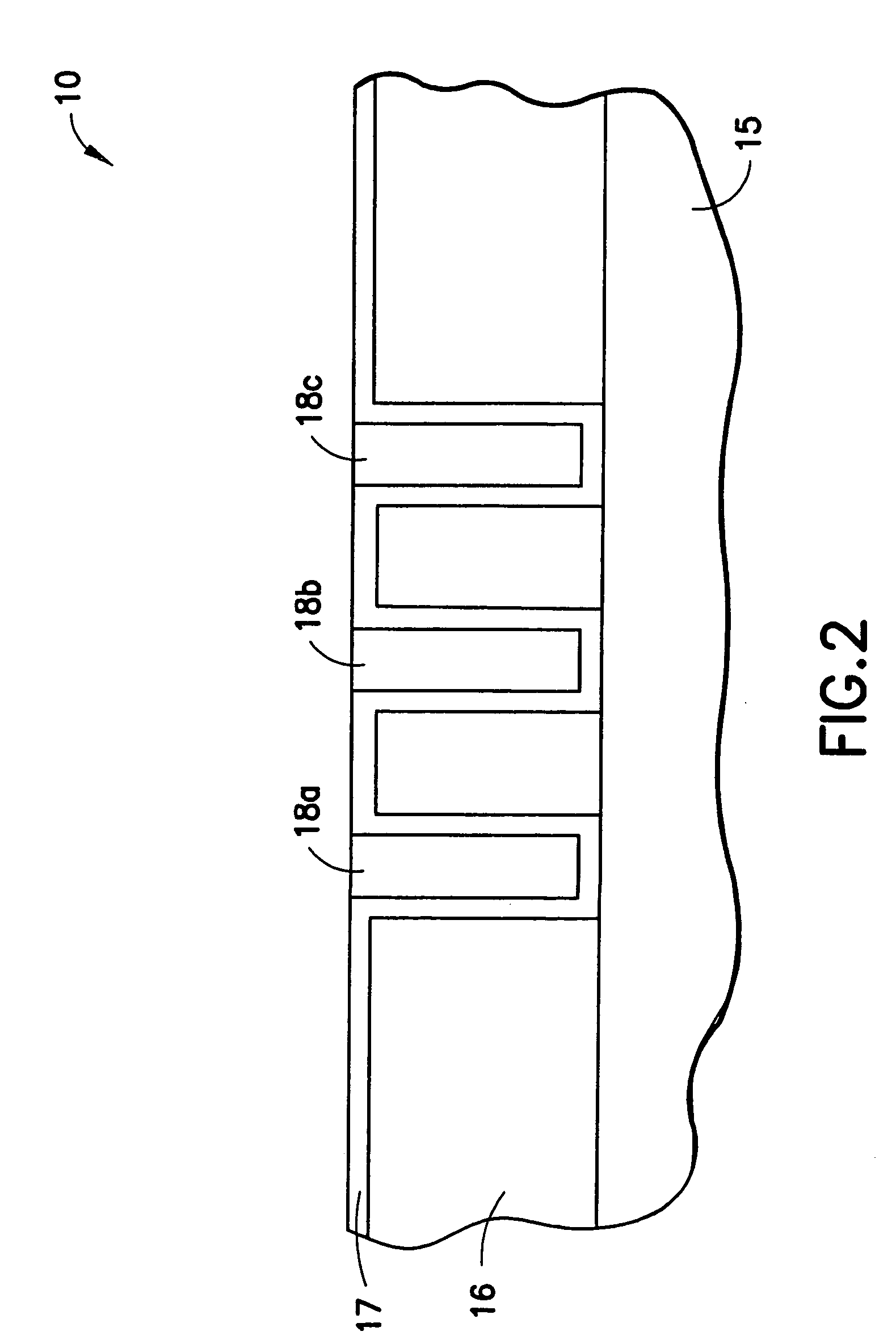
[0019] The present invention is directed to a chemical mechanical polishing slurry comprising a first slurry, which has a high removal rate on copper and a low removal rate on barrier material and a second slurry, which has a high removal rate on barrier material and a low removal rate on copper and the associated dielectric material. The first and second slurries comprise silica particles, an oxidizing agent, a corrosion inhibitor, and a cleaning agent. Also disclosed as the present invention is a method for chemical mechanical polishing copper, barrier material and dielectric material with the polishing slurry of the present invention. As will become apparent from the discussion that follows, the stable slurry and method of using the slurry provide for removal of material and polishing of semiconductor wafer surfaces with significantly no dishing or oxide erosion, with significantly no surface defects and good planarization efficiency, and produce a copper surface with minimal corrosion tendency post-polish.

Problems solved by technology

If appropriate material removal selectivity is not maintained, unwanted dishing of copper and / or erosion of the dielectric material may occur.
This disparity, in removal rates during the removal and polishing of the barrier material results in significant dishing of copper on the surface of the semiconductor wafer and / or poor removal of the barrier material.
Another problem with conventional CMP slurries is that the removal chemistry of the slurry is compositionally unstable.
Further, many of the colloidal abrasives agglomerate after relatively short time frames following addition to the supporting chemistry.
Both of these problems lead to significant operational obstacles.
A further problem in commercial CMP slurries is that the abrasive materials in the slurries produce defects in the form of micro scratches.
These slurries also have poor planarization efficiency, which is the ability of the slurry to polish high points preferentially over low points on the surface of the wafer.
Micro scratches and poor planarization efficiency result in integrated circuits with increased defects and a lower yield.
Still another problem of commercial CMP slurries is that the chemicals that make up the slurries produce a copper surface that has a high corrosion tendency post polish.

Method used


Image

  • Polishing slurries for copper and associated materials
  • Polishing slurries for copper and associated materials
  • Polishing slurries for copper and associated materials

Examples


example 1

[0042] Precipitated silica mean particle sizes of 8 nm, 20 nm, and 70 nm were tested. The fumed silica particle size tested was less than 700 nm. The optimum CMP slurry, including the first and second slurry, had a precipitated silica mean size of less than about 100 nm. The optimum fumed silica abrasive mean size for the first slurry is less than about 700 nm. The optimum CMP slurry formulations contain 1-10% precipitated silica, or fumed silica for the first slurry.

[0043] Further, different types of abrasive particles were studied to maximize the removal and selectivity characteristic of the slurry. Precipitated silica abrasives, with mean size distributions of 4 nm, 8 nm, 13 nm, 20 nm and 70 nm were tested. FIG. 6 shows a TEM picture of 13 nm slurry. The size distribution of these particles is presented in FIG. 7. Fumed silica, with a mean particle size of less than about 700 nm, was also evaluated. All of these mean size distributions can be used to achieve effective polishing ...

example 2

[0044] Different pH ranges were tested for the first and second slurries (See Table 2 and 3). The precipitated silica abrasives had a starting pH range of 9-11 and the fumed silica had a starting pH range of 2-7. The optimum CMP slurry was found to be acidic. Thus, the pH ranges were altered to the 2 to 5 range by adding potassium, sodium or ammonium hydroxide in appropriate amounts to solutions of iodic acid, cleaning agent and corrosion inhibitor.

example 3

[0045] Several formulations of the first slurries were prepared. The characteristics of these formulations are described in Table 2. The first slurry is optimally comprised of formula 5, for colloidal silica particles, and formula 19 for fumed silica particles. Thus, the first slurry is preferentially comprised of 1-10% colloidal silica with particle size 3 to 100 nm, or 1-5% fumed silica with mean particle size of less than about 700 nm. Further, the active chemistry for the optimum first slurry is about 1-12% potassium iodate (KIO3, formed by reaction of HIO3 with KOH), which is used as the oxidizing agent for the copper, about 0-5% concentrated inorganic acid as a copper activating agent, and 0-2% iminodiacetic acid (IDA) as the copper corrosion inhibitor and cleaning agent.

TABLE 2Formulations for the First SlurryCopperCopperThermalCopperTantalumTantalumFormulaOxidizer, %Inhibitor, %Activator, %Neutralizer, %Abrasive, %pHOxide RR *RR *RRNitride RR1HIO3. 8.22IDA, 1.5H3PO4 1.764K...


PUM

PropertyMeasurementUnit
weight ratioaaaaaaaaaa
weight percentaaaaaaaaaa
particle sizeaaaaaaaaaa

Abstract

A chemical mechanical polishing slurry and method for using the slurry for polishing copper, barrier material and dielectric material that includes a first and second slurry. The first slurry has a high removal rate on copper and a low removal rate on barrier material. The second slurry has a high removal rate on barrier material and a low removal rate on copper and dielectric material. The first and second slurries can include silica particles, an oxidizing agent, a corrosion inhibitor, and a cleaning agent.

Description

CROSS-REFERENCE TO RELATED APPLICATIONS [0001] This is a continuation of U.S. patent application Ser. No. 10 / 022,317 filed Dec. 18, 2001, which in turn is a division of U.S. patent application Ser. No. 09 / 562,698 filed May 1, 2000, issued Jun. 25, 2002 as U.S. Pat. No. 6,409,781.BACKGROUND OF THE INVENTION [0002] 1. Field of the Invention [0003] The present invention relates to a chemical mechanical polishing slurry for surfaces of a semiconductor wafer, and more particularly, to a chemical mechanical polishing slurry and a method for using the slurry to remove and polish copper, barrier materials and dielectric materials layered on semiconductor wafer surfaces. [0004] 2. Description of the Related Art [0005] Semiconductor wafers are used to form integrated circuits. The semiconductor wafer typically includes a substrate, such as silicon, upon which dielectric materials, barrier materials, and metal conductors and interconnects are layered. These different materials have insulating,...

Claims


Application Information

Patent Timeline
Patent Type & Authority Applications(United States)
IPC IPC(8): H01L21/461C09C1/68C09G1/02H01L21/321
CPCC09G1/02H01L21/3212
Inventor WOJTCZAK, WILLIAM A.BAUM, THOMAS H.NGUYEN, LONGREGULSKI, CARY
Owner CABOT MICROELECTRONICS CORP
Learn More