Double silicon-on-insulator (SOI) metal oxide semiconductor field effect transistor (MOSFET) structures

a metal oxide semiconductor and field effect transistor technology, applied in the field of semiconductor devices, to achieve the effect of reducing the step height and not penalizing the junction capacitan

Active Publication Date: 2006-04-25
GLOBALFOUNDRIES U S INC
View PDF12 Cites 36 Cited by
  • Summary
  • Abstract
  • Description
  • Claims
  • Application Information

AI Technical Summary

Benefits of technology

[0008]The present invention provides a structure and method that achieves SOI MOSFETs formed on a plurality of semiconductor layers (with independently selected material and thickness) all integrated in a single substrate. The structure of the present invention also allows for a thin insulator (thus reduced step height) between the semiconductor layers without penalizing the junction capacitance of the device to be fabricated on the upper semiconductor layer.

Problems solved by technology

One problem with the foregoing approaches is that there exists a step region (consisting of the various semiconductor layers) between the different types of device structures.

Method used


Image

  • Double silicon-on-insulator (SOI) metal oxide semiconductor field effect transistor (MOSFET) structures
  • Double silicon-on-insulator (SOI) metal oxide semiconductor field effect transistor (MOSFET) structures
  • Double silicon-on-insulator (SOI) metal oxide semiconductor field effect transistor (MOSFET) structures

Examples


Embodiment Construction

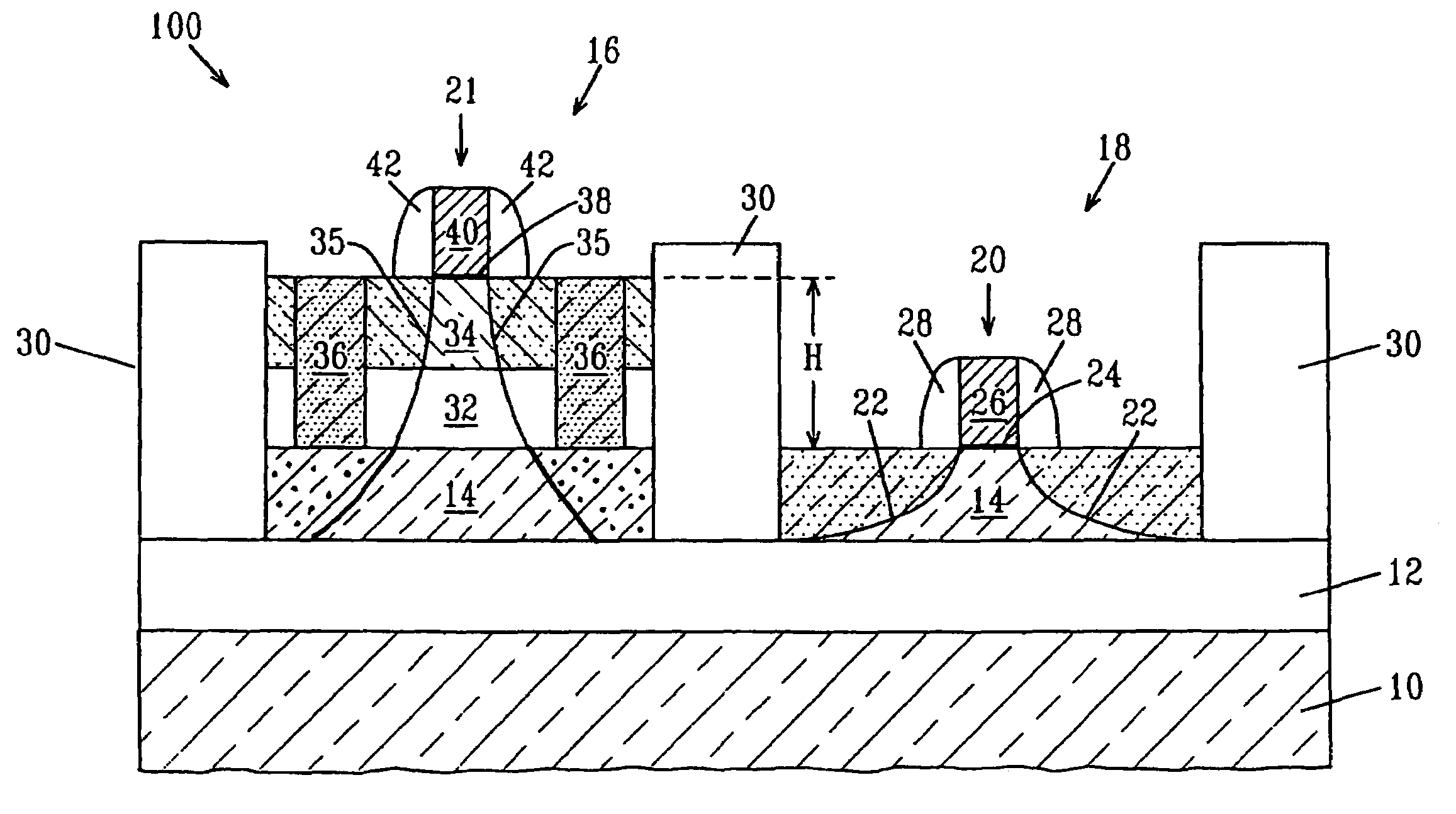
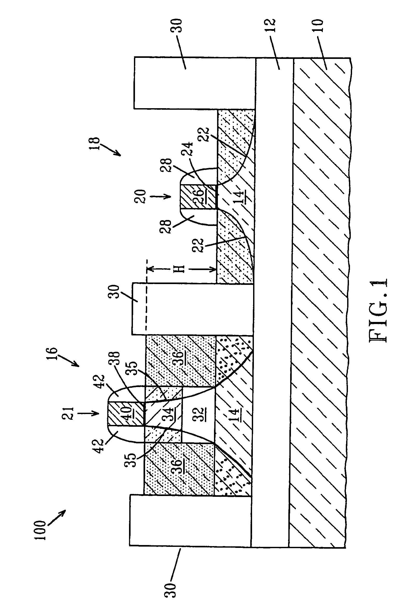
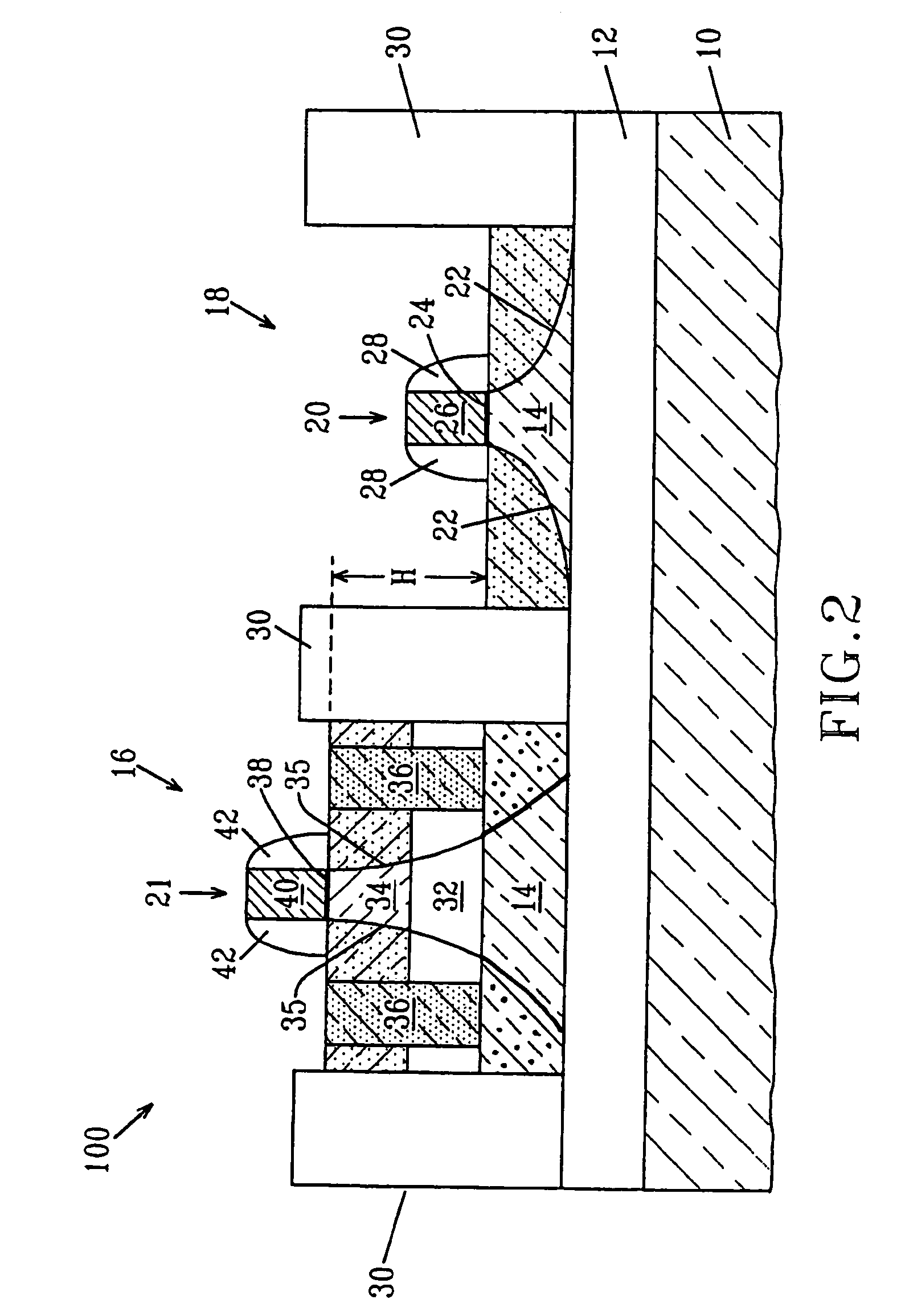
[0024]The present invention, which provides a double SOI MOSFET structure having a reduced step height between the various semiconductor layers, while not adversely affecting the junction capacitance of the semiconductor device located on the upper semiconductor layer, will now be described in greater detail by referring to the drawings that accompany the present application.

[0025]FIGS. 1 and 2 show cross sectional views of the double SOI MOSFET structure 100 of the present invention. Specifically, the double SOI MOSFET structure 100 of the present invention comprises semiconductor substrate 10, first buried insulating layer 12 located on an upper surface of the semiconductor substrate 10, first semiconductor layer 14 located on an upper surface of a portion of the first buried insulator layer 12, elevated device region 16 and recessed (relative to the elevated device region 16) device region 18. As shown, the recessed device region 18 is located directly on top of the first semicon...


PUM


Abstract

A SOI MOSFET structure having a reduced step height between the various semiconductor layers without adversely affecting the junction capacitance of the semiconductor device formed on the uppermost semiconductor layer as well as a method of fabricating the same are provided. The structure of the present invention includes an elevated device region having at least one semiconductor device located on a second semiconductor layer. The elevated device region further includes a source / drain junction that extends from the second semiconductor layer down to a first buried insulator layer that is located on an upper surface of the semiconductor substrate. The structure also includes a recessed device region having at least one semiconductor device located atop a first semiconductor layer which is located on an upper surface of the first buried insulator. An isolation region separates the elevated device region from the recessed device region.

Description

FIELD OF THE INVENTION[0001]The present invention relates to a semiconductor device and a method of fabricating the same, and more particularly to a double silicon-on-insulator (SOI) metal oxide semiconductor field effect transistor (MOSFET) structure and a method of fabricating such a structure.BACKGROUND OF THE INVENTION[0002]In the semiconductor industry, it is known to form nFETs and pFETs on semiconductor substrates that contain various heterolayers. Such technology is described, for example, in A. Sadek, et al. “Design of Si / SiGe Heterojunction Complementary Metal-Oxide-Semiconductor Transistors”, Electron Devices, IEEE Transactions, Vol. 43, Issue 8, August 1996, pp. 1224–1232. Specifically, an optimized Si / SiGe heterostructure for CMOS transistor operation is provided in the A. Sadek, et al. article which has a planar design and avoids inversion of the Si layer at the oxide interface.[0003]In such technology, the basic idea is to form a plurality of layers in a single struct...

Claims


Application Information

Patent Timeline
Patent Type & Authority Patents(United States)
IPC IPC(8): H01L27/12H01L21/84H01L29/04H01L29/10H01L29/786
CPCH01L21/84H01L27/1203H01L29/1054H01L29/045H01L29/78684H01L29/78681H01L21/76254H01L21/76283
Inventor RIM, KERN
Owner GLOBALFOUNDRIES U S INC
Why Eureka
Try Eureka