False-lock-free delay locked loop circuit and method

a delay lock and loop technology, applied in the field of false lock-free delay lock circuits, can solve the problems of compromising the “robustness” of the loop operation described in u.s. patent no. 6,239,634, and monitoring circuitry and associated correction circuitry designed for use in conjunction with a particular delay line usually would not be usable for a different delay line having a different number of delay cells without extensive modification

Active Publication Date: 2006-04-25
SAMSUNG ELECTRONICS CO LTD +1
View PDF3 Cites 21 Cited by
  • Summary
  • Abstract
  • Description
  • Claims
  • Application Information

AI Technical Summary

Benefits of technology

[0024]It is an object of invention to provide a DLL circuit that avoids false-lock conditions.
[0025]It is another object of the invention to provide a DLL circuit that readily automatically recovers from false-lock conditions.
[0026]It is another object of the invention to provide a DLL circuit that avoids the need to provide additional circuitry to preset or clamp the output voltage of a loop filter circuit in order to enable the DLL circuit to reliably establish and / or maintain a correct lock condition.
[0027]It is another object of the invention to provide a DLL circuit that avoids the need for a reset operation in order to ensure a correct lock condition.
[0028]It is another object of the invention to provide a DLL circuit that avoids the need to provide a monitoring circuit to take over charging or discharging of the loop filter capacitor until the DLL feedback loop is able to take over and reliably establish a correct lock condition.
[0030]There also is an unmet need for a DLL circuit including a phase detector having substantially increased information monitoring capability to monitor the status of progression of a reference clock polls through the delay line of the DLL and use that information to avoid false-lock conditions.

Problems solved by technology

A problem of the conventional DLL of FIG. 1 is that it may try to “lock onto” an incorrect pulse that is delayed by an integer number nT of periods of the input clock, where n is greater than 1.
Such a false-lock condition usually is an undesirable condition, especially if it persists, because it would produce unintended signal delays, which would be likely to cause circuit malfunctions and sometimes may have disastrous results.
A problem with this approach is that the value at which to pre-set the loop filter output voltage must be known.
This makes it difficult to provide the preset or clamp value of the loop filter output voltage to with a preset or clamp value that can cause the loop to reliably lock on the correct rising edge of the output voltage dN of the last delay cell.
If the prior art DLL 20 is ever caused to be in a false-lock condition, there is no mechanism to allow the feedback loop to recover to a correct lock condition.
Unfortunately, the “robustness” of the loop operation described in U.S. Pat. No. 6,239,634 is compromised because a correct lock condition can only be guaranteed by performing a reset operation.
Also, the monitoring circuitry and associated correction circuitry designed for use in conjunction with a particular delay line usually would not be usable for a different delay line having a different number of delay cells without extensive modification.

Method used


Image

  • False-lock-free delay locked loop circuit and method
  • False-lock-free delay locked loop circuit and method
  • False-lock-free delay locked loop circuit and method

Examples


Embodiment Construction

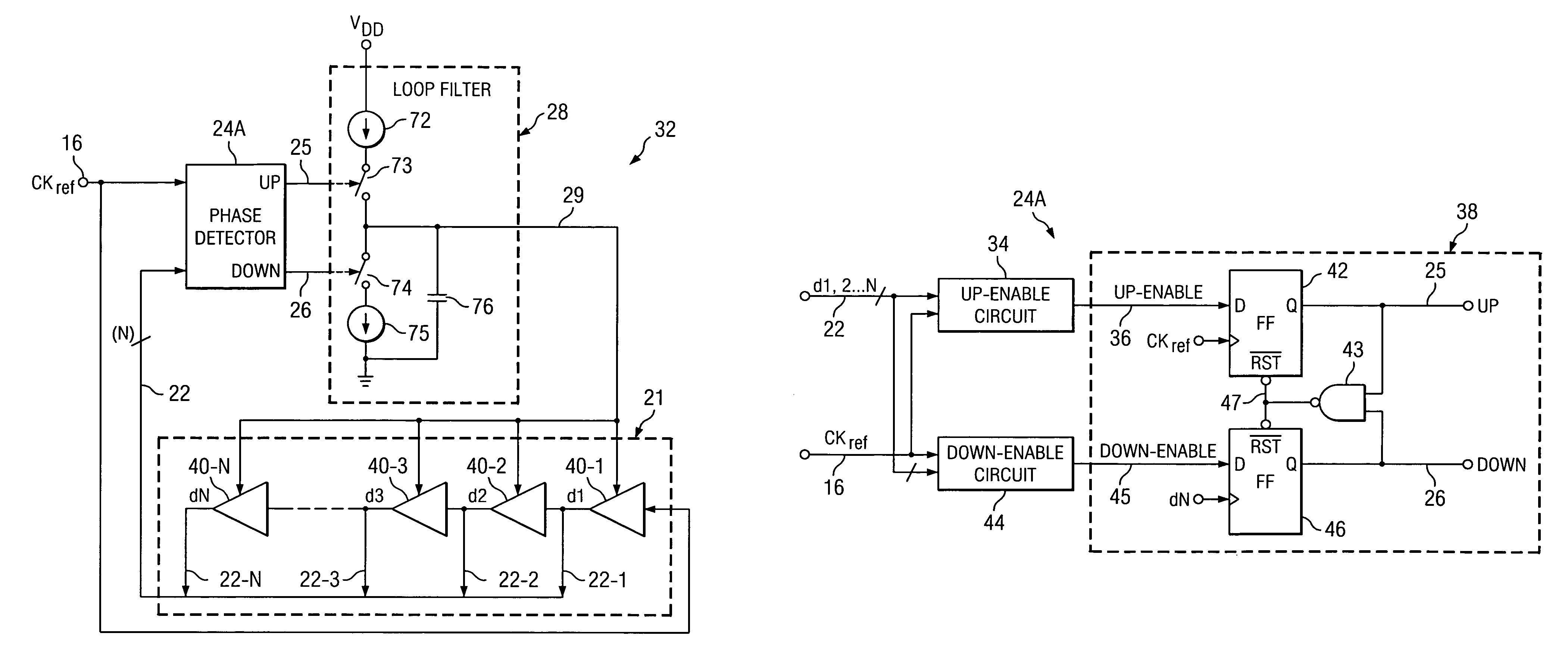
[0044]The present invention solves the above mentioned problems of the prior art by building more capability into the phase detector of a DLL circuit. Instead of comparing only the output of the last delay cell of the delay line with the reference clock signal CKref, a plurality of or all of the delay cell output signals are provided as inputs to the phase detector. This allows it to utilize information regarding the status of propagation of a pulse of the reference clock signal CKref through the delay line in a way that avoids sustained false-lock conditions.

[0045]Referring to FIG. 4, a false-lock-free DLL 32 includes the same delay line 21 and loop filter circuit 28 shown in “prior art”FIG. 1. False-lock-free DLL 32 includes a phase detector 24A having its clock input coupled to CKref. As in prior art FIG. 1, delay line 21 includes N delay cells 40-1, 40-2 . . . 40-N, wherein each delay cell includes a delay control input connected to delay control conductor 29. The outputs of del...


PUM


Abstract

A phase detector in a delay locked loop circuit operates to determine the status of propagation of a first pulse of a reference clock signal (CKref) through a delay line (21). A first control signal (DOWN) is produced a in response to represent a first time at which the first pulse has progressed entirely through the delay line (21) and a later second time at which a next second pulse of the reference clock signal (CKref) arrives at a first input of the phase detector (24A). The delay of the delay line (21) is reduced in response to the first control signal (DOWN). A second control signal (UP) is produced in response to the status to represent a third time at which the second pulse of the reference clock signal (CKref) arrives at the first input of the phase detector (24A) and a later fourth time at which the first pulse of the reference clock signal (CKref) has progressed to the end of the delay line (21) and is used to increase the delay of the delay line (21).

Description

BACKGROUND OF THE INVENTION[0001]The present invention relates generally to delay locked loop (DLL) circuits, and more particularly to circuitry for providing “false-lock-free” phase comparison in a delay locked loop circuit.[0002]Delay locked loops (DLLs) are widely used in analog circuit design. The capability of a DLL to provide timing of clock signals that are precisely delayed relative to a reference clock signal is very valuable in many applications, such as circuits for eliminating clock skew, multi-phase clock generators, and clock / data recovery circuitry.[0003]FIG. 1 shows a conventional delay locked loop circuit 20 including a delay line 21. Delay line 21 includes N delay cells 40-1, 40-2 . . . 40-N as shown, wherein each delay cell includes a delay control input connected to delay control conductor 29. A reference clock CKref is applied as an input to the first delay cell 40-1 and a first input of a phase detector 24. The output d1 of the first delay cell 40-1 is connecte...

Claims


Application Information

Patent Timeline
Patent Type & Authority Patents(United States)
IPC IPC(8): H03L7/06
CPCH03L7/0891H03L7/0812H03L7/0816
Inventor WANG, BINAN
Owner SAMSUNG ELECTRONICS CO LTD
Why Eureka
Try Eureka