Dual gate structure for a FET and method for fabricating same

a gate structure and gate technology, applied in the field of field effect transistors, can solve the problems of increasing leakage current, increasing channel length, and low supply voltage between the drain and the source, so as to improve the control of the vertical characteristics of the gate structure, reduce the effective channel length, and reduce the parasitic capacitance

Inactive Publication Date: 2006-05-02
POWER INTEGRATIONS INC
View PDF43 Cites 32 Cited by
  • Summary
  • Abstract
  • Description
  • Claims
  • Application Information

AI Technical Summary

Benefits of technology

[0014]Accordingly, embodiments of the present invention provide enhanced control over the vertical characteristics of gate structures of JFETs and MESFETs. In embodiments of the present invention, multiple ion implantation steps are used to provide a dual gate structure that reduces the effective channel length, leakage current, and parasitic capacitance in JFETs and MESFETs.

Problems solved by technology

However, the supply voltage between the drain and source (Vds) is usually relatively low when the device is turned on.
For vertical FET devices, the lack of close control over the device characteristics in the vertical dimension results in longer channel lengths, increased leakage current, and increased parasitic capacitance.

Method used


Image

  • Dual gate structure for a FET and method for fabricating same
  • Dual gate structure for a FET and method for fabricating same
  • Dual gate structure for a FET and method for fabricating same

Examples


Embodiment Construction

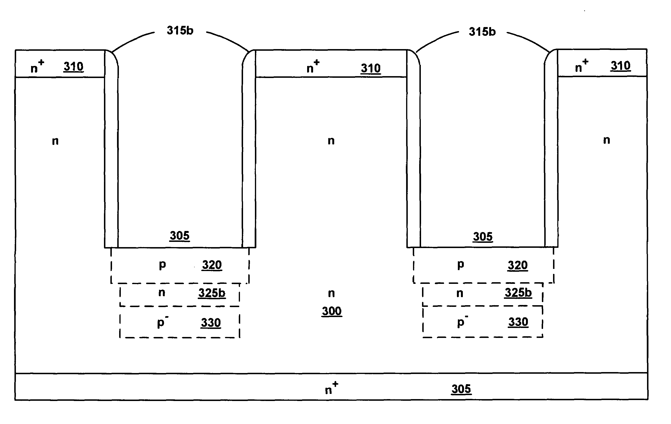
[0028]In the following detailed description of the present invention, a dual gate structure and a method for fabricating the structure; numerous specific details are set forth in order to provide a thorough understanding of the present invention. However, it will be obvious to one skilled in the art that the present invention may be practiced without these specific details. In other instances well known methods involving photolithography, ion implantation, deposition and etch, etc., and well known structures such as ohmic contacts and barrier metallization, etc., have not been described in detail so as not to unnecessarily obscure aspects of the present invention.

[0029]U.S. patent applications Ser. No. 10 / 158,326, “Method and Structure for Reduced Gate Capacitance,” (filed May 29, 2002) and Ser. No. 10 / 191,030 “Method and Structure for Double Dose Gate in a JFET,” (filed Jul. 2, 2002), are assigned to the assignee of the present invention and describe gate structures and methods of ...


PUM


Abstract

A method for fabricating a dual gate structure for JFETs and MESFETs and the associated devices. Trenches are etched in a semiconductor substrate for fabrication of a gate structure for a JFET or MESFET. A sidewall spacer may be formed on the walls of the trenches to adjust the lateral dimension for a first gate. Following the formation of the first gate by implantation or deposition, a buffer region is implanted below the first gate using a complementary dopant and a second sidewall spacer with a thickness that may be the same or greater than the thickness of the first sidewall spacer. Subsequent to the buffer implant, a second gate is implanted beneath the buffer layer using a third sidewall spacer with a greater thickness than the first sidewall spacer.

Description

FIELD OF THE INVENTION[0001]Embodiments of the present invention relate to field effect transistors (FETs). In particular, embodiments of the present invention relate to a gate structure for improved performance characteristics in FETs.BACKGROUND ART[0002]Junction field effect transistors (JFETs) are majority carrier devices that conduct current through a channel that is controlled by the application of a voltage to a p-n junction. JFETs may be constructed as p-channel or n-channel and may be operated as enhancement mode devices or depletion mode devices. Similar to the JFET is the metal-semiconductor field effect transistor (MESFET). In MESFETs, a junction between a metal and a semiconductor is used to create a Schottky barrier that takes the place of the p-n junction of the JFET.[0003]The most common JFET type is the depletion mode type. The depletion mode device is a “normally on” device that is turned off by reverse biasing the p-n junction so that pinch-off occurs in the conduc...

Claims


Application Information

Patent Timeline
Patent Type & Authority Patents(United States)
IPC IPC(8): H01L29/80H01L31/112
CPCH01L29/66848H01L29/66909H01L29/8128H01L29/8124H01L29/8083
Inventor YU, HO-YUAN
Owner POWER INTEGRATIONS INC
Why Eureka
Try Eureka