Air gap interconnect structure and method of manufacture

a technology of interconnect structure and air gap, which is applied in the direction of semiconductor devices, semiconductor/solid-state device details, electrical apparatus, etc., can solve the problems of time delay, cross-talk between wiring elements, and the final performance of the final semiconductor produ

Inactive Publication Date: 2006-05-09
IBM CORP
View PDF8 Cites 79 Cited by
  • Summary
  • Abstract
  • Description
  • Claims
  • Application Information

AI Technical Summary

Benefits of technology

[0022]An advantage of the present invention is that polymer gap fill can be removed simultaneously with (in the same step as) creating the capping layer. Another advantage is the ability to pattern the top layer using a photosensitive polymer.
is that polymer gap fill can be removed simultaneously with (in the same step as) creating the capping layer. Another advantage is the ability to pattern the top layer using a photosensitive polymer.

Problems solved by technology

Resulting capacitance increase produces time delays and creates cross-talk between the wiring elements.
RC (resistance-capacitance resonant) losses in the wiring levels of integrated circuits (ICs) make significant contributions limiting the final performance of the final semiconductor product.
The reaction products escape through the porous air-bridge resulting in air-filled gaps.

Method used


Image

  • Air gap interconnect structure and method of manufacture
  • Air gap interconnect structure and method of manufacture
  • Air gap interconnect structure and method of manufacture

Examples


Embodiment Construction

[0026]In the description that follows, numerous details are set forth in order to provide a thorough understanding of the present invention. It will be appreciated by those skilled in the art that variations of these specific details are possible while still achieving the results of the present invention. Well-known processing steps are generally not described in detail in order to avoid unnecessarily obfuscating the description of the present invention.

[0027]In the description that follows, exemplary dimensions are presented for an illustrative embodiment of the invention. The dimensions should not be interpreted as limiting. They are included to provide a sense of proportion. Generally speaking, it is the relationship between various elements, where they are located, their contrasting compositions, and sometimes their relative sizes that is of significance.

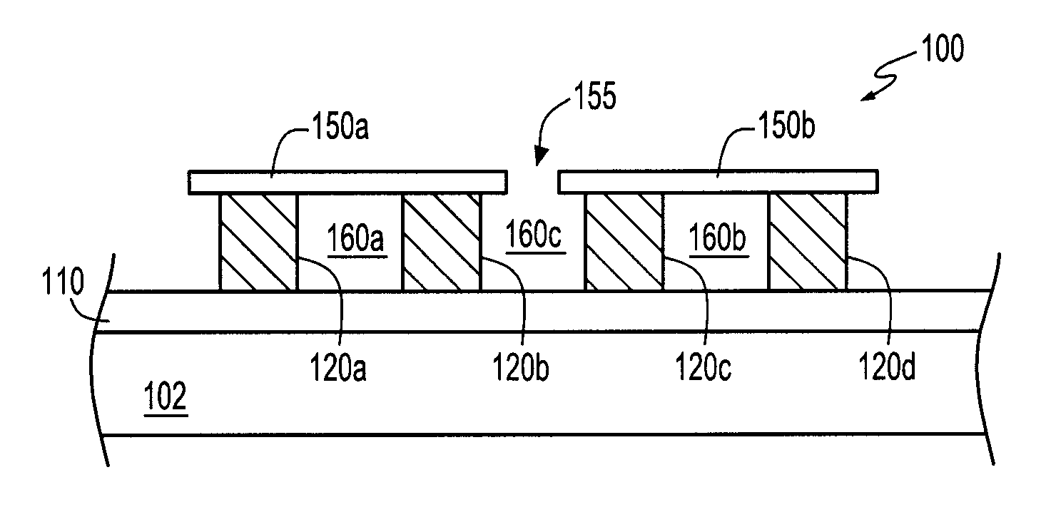
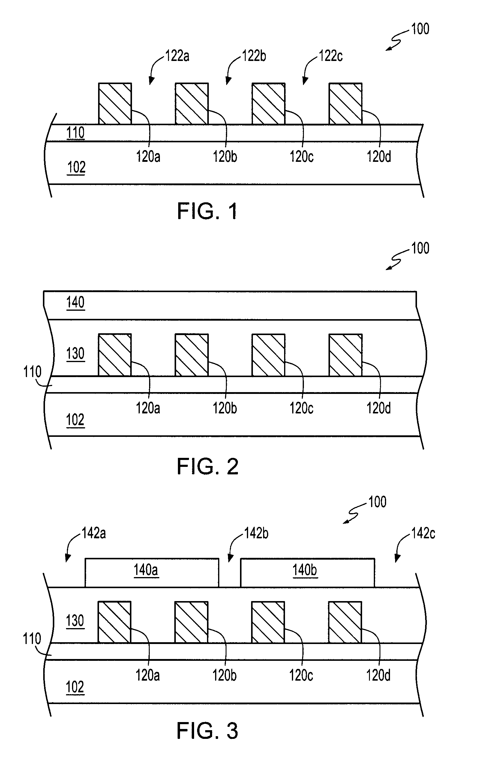
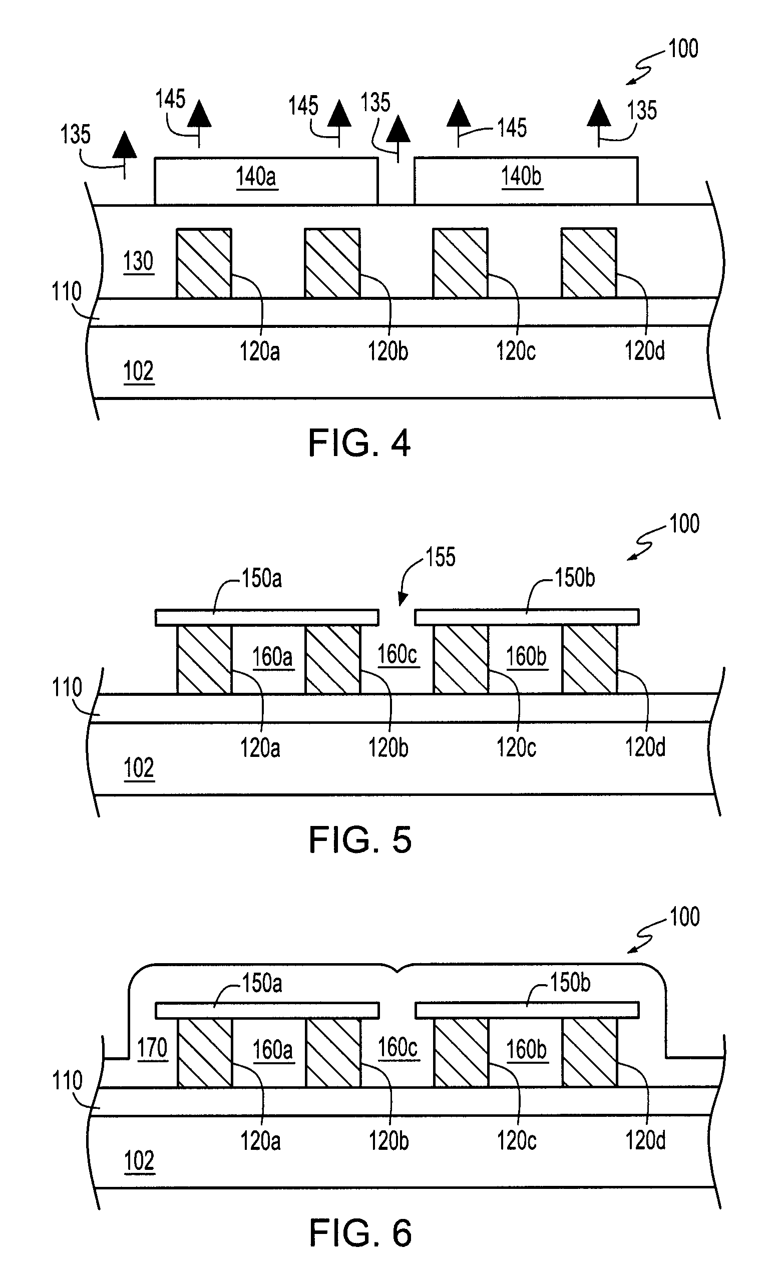
[0028]FIGS. 1–6 illustrate a first embodiment of the invention. FIGS. 7–11 illustrate a second embodiment of the invention. In...


PUM


Abstract

A dual layer of polymeric material is deposited with a base layer and top layer resist onto an integrated circuit structure with topography. The base layer planarizes the surface and fills in the native topography. The base layer decomposes almost completely when exposed to an oxidizing environment. The top layer contains a high composition of oxidizing elements and is photosensitive. (i.e., the layer can be patterned by exposing normal lithographic techniques.) The patterning allows the creation of escape paths for the decomposition products of the underlying base layer. This structure is decomposed in an oxidizing ambient (or plasma) leaving behind a thin carbon-containing membrane. This membrane layer blocks deposition of future layers, creating air gaps in the structure.

Description

BACKGROUND OF INVENTION[0001]The present invention relates generally to semiconductor device processing and, more particularly to interconnect structures having air gaps between adjacent conductive lines.[0002]The evolution of integrated circuits toward higher complexity and decreased size has lead to closer spacing between the conducting wires (lines). Resulting capacitance increase produces time delays and creates cross-talk between the wiring elements. Current semiconductor fabrication techniques typically comprise many conductive wiring levels to complete the final working integrated circuits.[0003]Semiconductor devices are typically joined together to form useful circuits using what is called “interconnect structures.” These interconnect structures are typically made of conductors such as copper (Cu) or aluminum (Al) and dielectric materials such as silicon dioxide (SiO2). The speed of these interconnects can be roughly assumed to be inversely proportional to the product of the...

Claims


Application Information

Patent Timeline
Patent Type & Authority Patents(United States)
IPC IPC(8): H01L21/76H01L21/768H01L21/8242H01L23/522
CPCH01L21/7682H01L23/5222H01L2924/0002H01L2924/00
Inventor STRANE, JAY W.
Owner IBM CORP
Why Eureka
Try Eureka