MRAM cell structure and method of fabrication

a technology of mram cell and cell structure, applied in the direction of digital storage, instruments, semiconductor devices, etc., can solve the problems of poor device performance and device performance degradation

Active Publication Date: 2006-05-16
TAIWAN SEMICON MFG CO LTD
View PDF20 Cites 137 Cited by
  • Summary
  • Abstract
  • Description
  • Claims
  • Application Information

AI Technical Summary

Benefits of technology

[0014]One objective of the present invention is to provide an MRAM cell structure in which the distance between a bit line or a word line and an underlying free layer in a magnetic tunnel junction is well controlled.

Problems solved by technology

Unfortunately, two major issues lead to a degradation of device performance.
Because the magnetic field strength generated by the bit line or word line current at the free layer strongly depends on the distance (t1−t2), the inability to control this parameter directly translates to a failure to control the switching magnetic field at the free layer and thereby leads to poor device performance.
A second problem is that the CMP process often forms an MTJ 4 that protrudes above the surrounding insulation layer 5 by a distance d. The protrusion distance d varies across a wafer and from wafer to wafer because of the same nonuniformities mentioned previously.

Method used


Image

  • MRAM cell structure and method of fabrication
  • MRAM cell structure and method of fabrication
  • MRAM cell structure and method of fabrication

Examples


Embodiment Construction

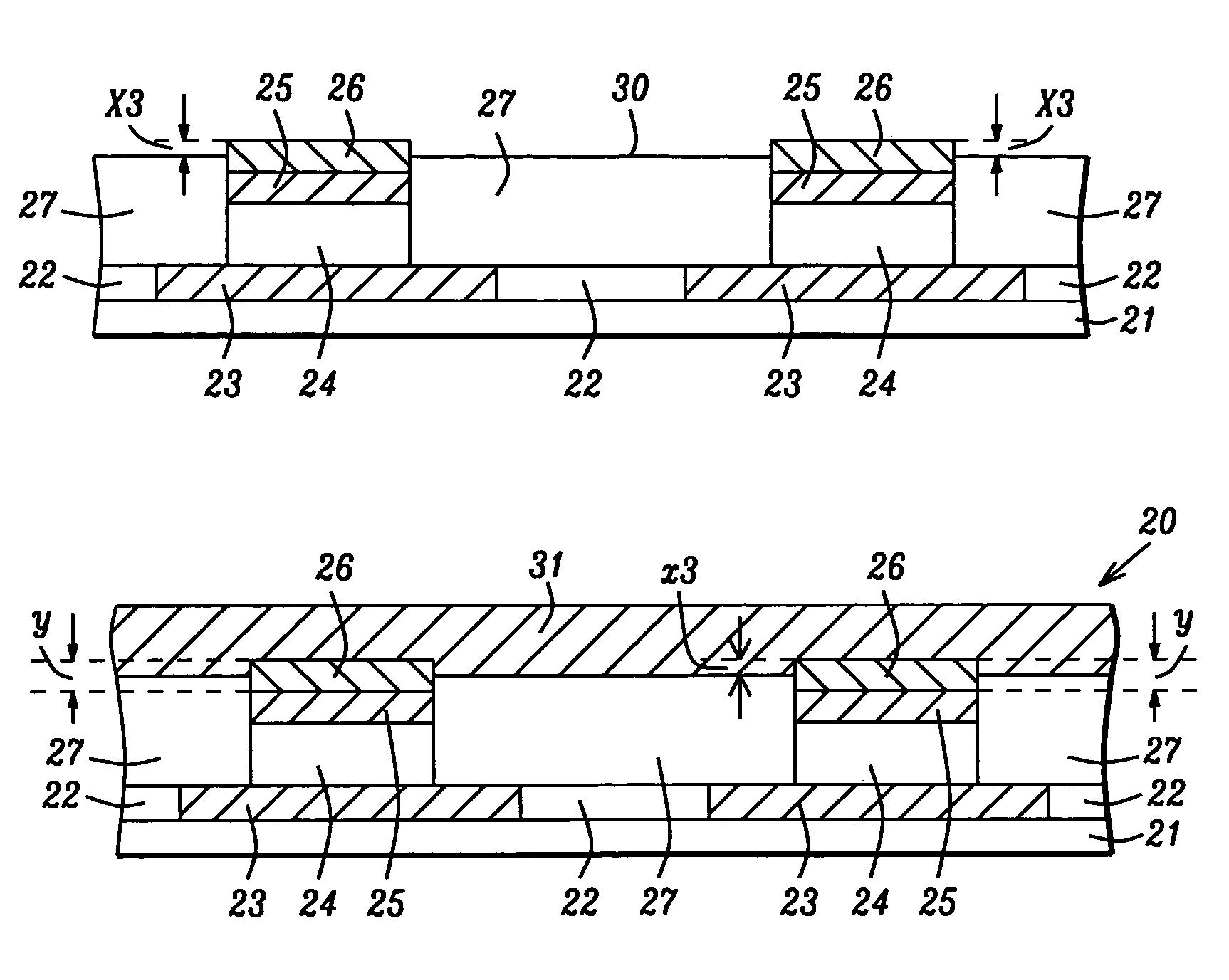
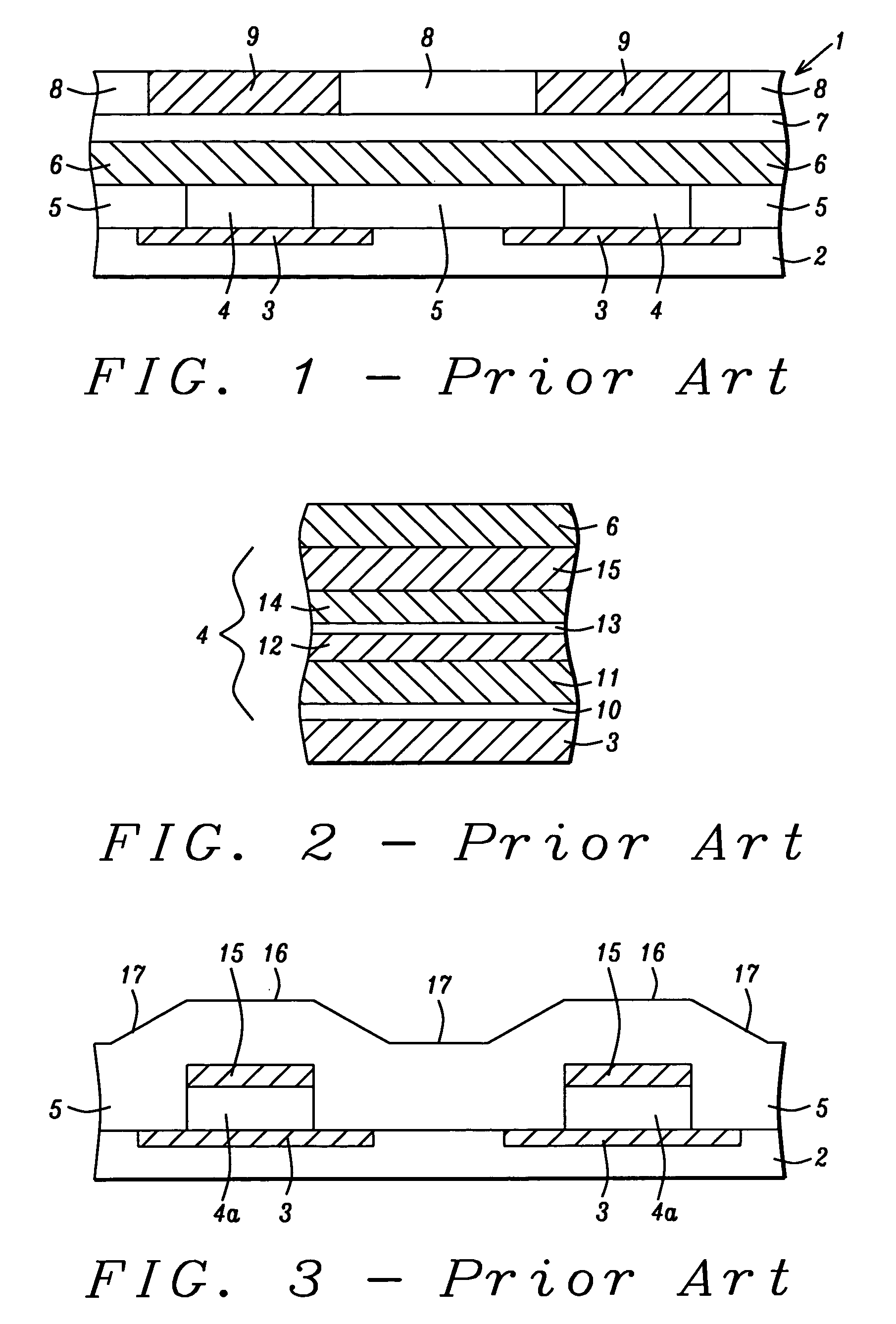
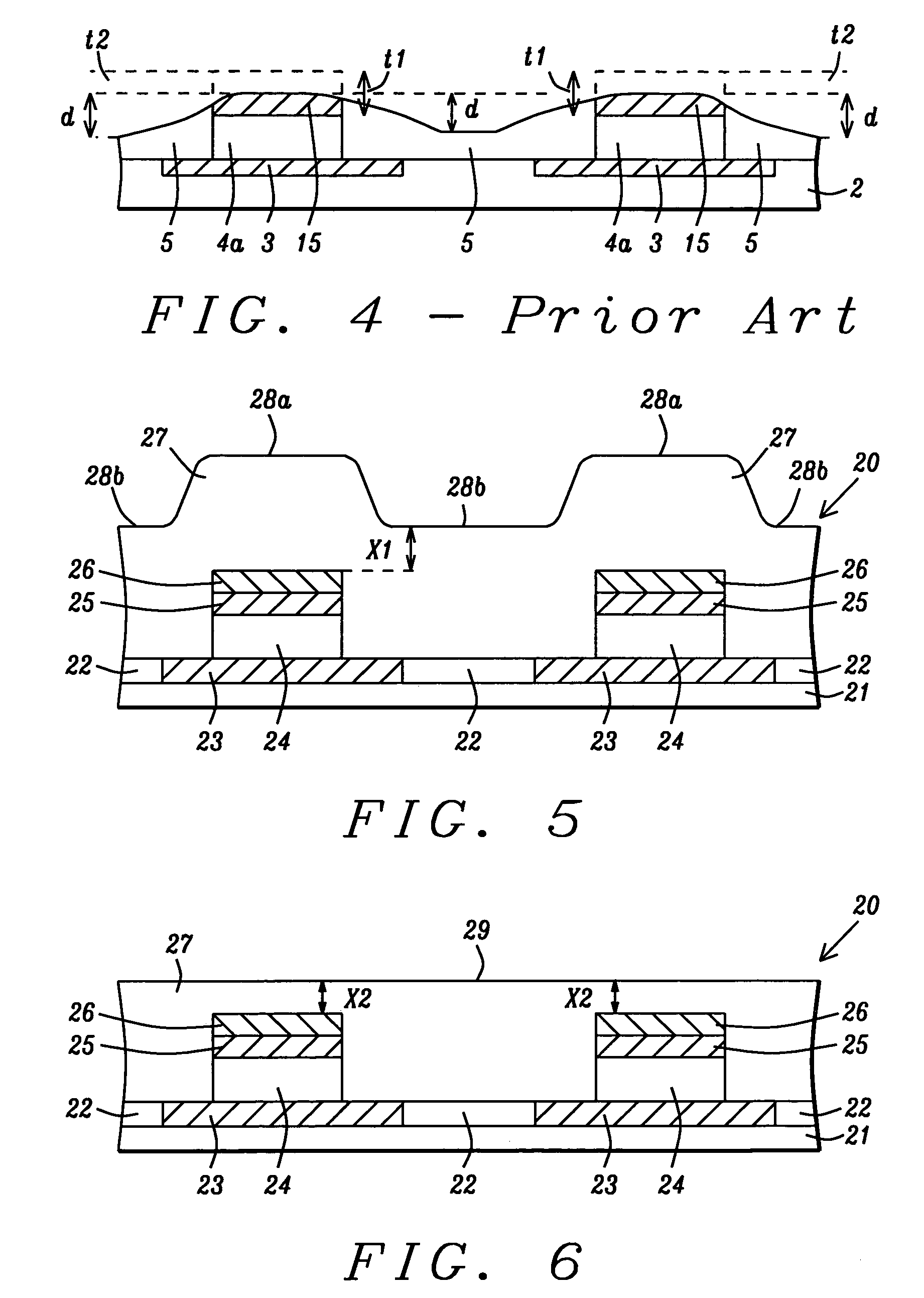
[0031]The present invention is an MRAM cell structure on an MRAM chip in which the distance from a bit line or word line to an underlying free layer in a magnetic tunnel junction (MTJ) is well controlled and an adjacent insulation layer is essentially flat and coplanar with the MTJ. The drawings are provided by way of example and are not intended to limit the scope of the invention. Although only two MRAM cells and two MTJs are depicted in the cross-sectional drawings, it is understood that from a top-down view there are a plurality of MRAM cells in an array that includes multiple rows and multiple columns on the MRAM chip. MRAM cell structure is intended to mean a portion of the MRAM chip including the MTJ as well as nearby insulation layers and conductive layers.

[0032]A method of forming the MRAM cell structure of the present invention will be described first. Referring to FIG. 5, a partially completed MRAM cell structure 20 is shown that includes a substrate 21 which may be silic...


PUM


Abstract

An MRAM structure is disclosed where the distance from a bit line or word line to an underlying free layer in an MTJ is small and well controlled. As a result, the bit line or word line switching current is reduced and tightly distributed for better device performance. A key feature in the method of forming the MRAM cell structure is a two step planarization of an insulation layer deposited on the MTJ array. A CMP step flattens the insulation layer at a distance about 60 to 200 Angstroms above the cap layer in the MTJ. Then an etch back step thins the insulation layer to a level about 50 to 190 Angstroms below the top of the cap layer. Less than 5 Angstroms of the cap layer is removed. The distance variation from the free layer to an overlying bit line or word line is within + / −5 Angstroms.

Description

FIELD OF THE INVENTION[0001]The invention relates to an MRAM cell structure, and more particularly, to an MRAM cell structure in which the distance from a bit line or word line to a free layer in a magnetic tunnel junction is well controlled by implementing a planarization process that includes a chemical mechanical polish (CMP) step and an etch back step.BACKGROUND OF THE INVENTION[0002]A magnetic random access memory (MRAM) device is generally comprised of an array of parallel first conductive lines on a horizontal plane, an array of parallel second conductive lines on a second horizontal plane spaced above and formed in a direction perpendicular to the first conductive lines, and a magnetic tunnel junction (MTJ) formed at each location where a second conductive line crosses over a first conductive line. A first conductive line may be a word line while a second conductive line is a bit line or vice versa. Alternatively, the first conductive line may be a sectioned line which is a ...

Claims


Application Information

Patent Timeline
Patent Type & Authority Patents(United States)
IPC IPC(8): H01L21/00G11C11/16H01L27/22H01L43/12
CPCG11C11/16H01L27/222H01L43/12H10B61/00H10N50/01
Inventor HONG, LIUBOZHONG, TOMYANG, LIN
Owner TAIWAN SEMICON MFG CO LTD
Why Eureka
Try Eureka