Supercharge Your Innovation With Domain-Expert AI Agents!

Semiconductor integrated circuit device including OTP memory, and method of programming OTP memory

a technology of integrated circuit device and memory, which is applied in the direction of semiconductor devices, digital storage, instruments, etc., can solve the problems of requiring a test cost for the purpose, the ratio of the area occupied by the laser fuse is gradually increasing, and the inability to use the laser fus

Inactive Publication Date: 2006-05-16
KK TOSHIBA
View PDF10 Cites 58 Cited by
  • Summary
  • Abstract
  • Description
  • Claims
  • Application Information

AI Technical Summary

Benefits of technology

This approach enables the detection of marginal characteristics as defective bits, improving yield and reliability by efficiently verifying and reprogramming imperfectly programmed bits, thus enhancing the testing efficiency and reliability of OTP memory.

Problems solved by technology

This laser fuse ROM requires a special fuse blowing device and a blowing step using the device, and hence requires a test cost for the purpose.
Therefore, micropatterning of the laser fuse does not keep pace with that of the rest of the circuit, so the ratio of the area occupied by the laser fuse is gradually increasing.
Accordingly, the laser fuse cannot be used in, e.g., remedy of defects in a high-speed test after packaging, or built-in self repair performed by a test circuit built in a chip.
Unfortunately, embedding a nonvolatile memory which stores electric charge in a floating gate requires additional masks and processes for the purpose, and this increases the cost.
In the electrical fuse which thus uses a breakdown phenomenon as a program mechanism, programming is a stochastic process; some elements are programmed immediately after the application of stress, and some elements are not well programmed within a limited programming time.
However, the conventional verify determines pass / fail by executing the same sense operation as a normal operation, and hence cannot detect a bit having marginal characteristics as a defect.
This may cause a market defect.

Method used


Image

  • Semiconductor integrated circuit device including OTP memory, and method of programming OTP memory
  • Semiconductor integrated circuit device including OTP memory, and method of programming OTP memory
  • Semiconductor integrated circuit device including OTP memory, and method of programming OTP memory

Examples


Embodiment Construction

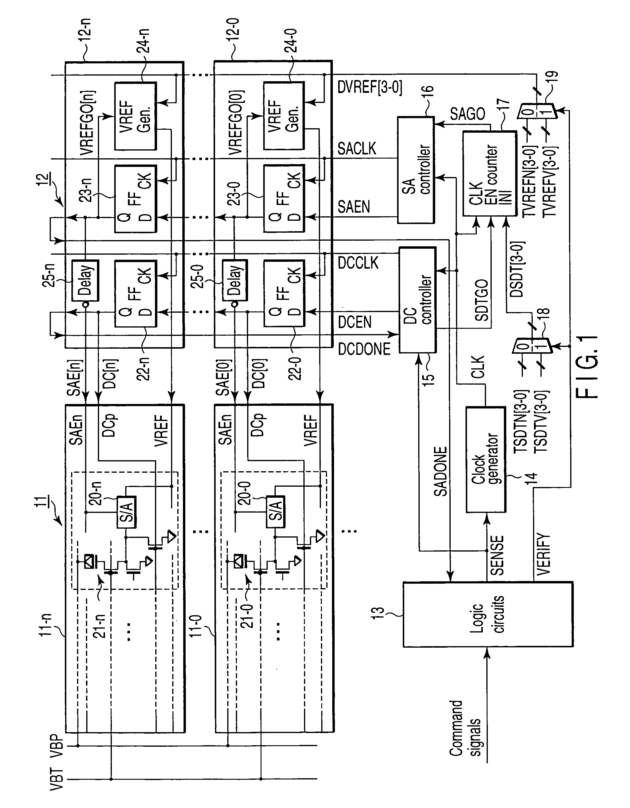
[0025]In an embodiment of the present invention, data corresponding to a programmed electrical fuse is “1”, and data corresponding to an electrical fuse which is not programmed is “0”. When verify is performed after an OTP memory using an electrical fuse is programmed, the margin of sensing data “1” in verify sense, in which data at the electrical fuse is read, is made smaller than that applied in a normal sense operation. Accordingly, even a bit having marginal characteristics can be sensed as a defective bit.

[0026]Data programmed at an electrical fuse is converted into a voltage at a level corresponding to the resistance of the electrical fuse. This voltage is compared with a reference voltage, and read out as “0” or “1”. When a signal voltage is generated by charging or discharging of a capacitor via an electrical fuse, the signal amount of data “1” can be controlled by changing the charging or discharging time. It is also possible to change the signal amount of data “1” viewed f...


PUM


Abstract

A semiconductor integrated circuit device includes a storage element, state sensing circuit, and control circuit. Information is programmed in the storage element by electrically irreversibly changing the element characteristics. The state sensing circuit is configured to sense the irreversibly changed state of the storage element in distinction from an unchanged state. The control circuit is configured to change the sensibility of the state sensing circuit.

Description

CROSS-REFERENCE TO RELATED APPLICATIONS[0001]This application is based upon and claims the benefit of priority from prior Japanese Patent Application No. 2004-113440, filed Apr. 7, 2004, the entire contents of which are incorporated herein by reference.BACKGROUND OF THE INVENTION[0002]1. Field of the Invention[0003]The present invention relates to a semiconductor integrated circuit device and a method of programming the same and, more particularly, to a semiconductor integrated circuit device including an electrically programmable irreversible storage element, i.e., a so-called OTP (One-Time Programmable) memory, and a method of programming information in this storage element.[0004]2. Description of the Related Art[0005]In the recent semiconductor integrated circuit devices, a nonvolatile OTP memory, in which stored information does not disappear even when the power supply is turned off, is an essential element. The OTP memory is widely used for the purposes of, e.g., redundancy of ...

Claims


Application Information

Patent Timeline
Patent Type & Authority Patents(United States)
IPC IPC(8): G11C7/00G11C17/00G11C8/00G11C16/06G11C17/12G11C17/16G11C17/18H10B69/00
CPCG11C17/18G11C17/16G11C7/1078G11C29/04
Inventor ITO, HIROSHINAMEKAWA, TOSHIMASA
Owner KK TOSHIBA
Features
  • R&D
  • Intellectual Property
  • Life Sciences
  • Materials
  • Tech Scout
  • Unparalleled Data Quality
  • Higher Quality Content
  • 60% Fewer Hallucinations
Learn More