Circuit board structure embedded with semiconductor chips
a technology of circuit board and semiconductor chips, applied in the direction of printed circuit manufacturing, printed circuit aspects, basic electric elements, etc., can solve the problems of high frequency operation, complex manufacturing process of semiconductor devices, and severe restrictions on the electric characteristics of semiconductor devices, so as to improve the electric characteristics of products
- Summary
- Abstract
- Description
- Claims
- Application Information
AI Technical Summary
Benefits of technology
Problems solved by technology
Method used
Image

Examples
first embodiment
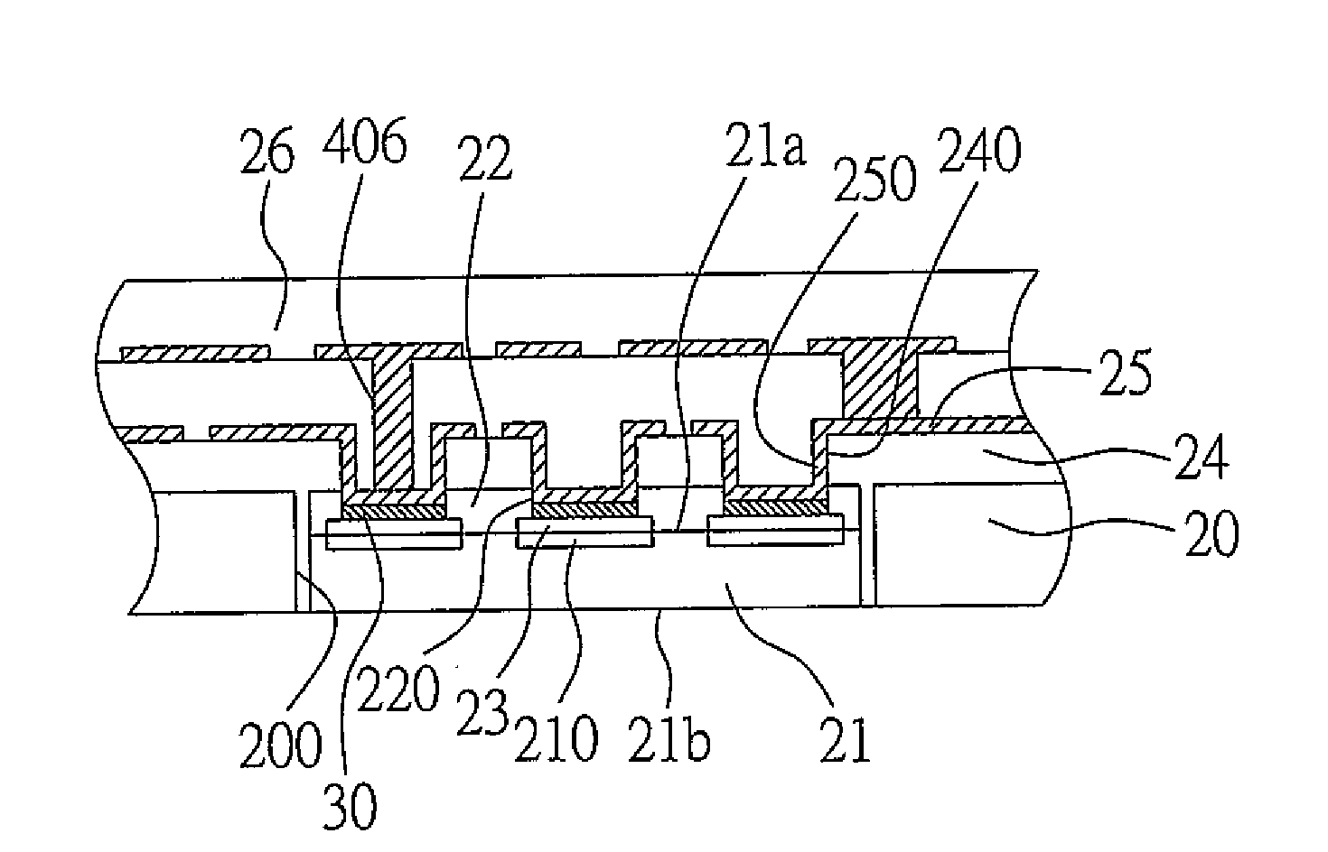
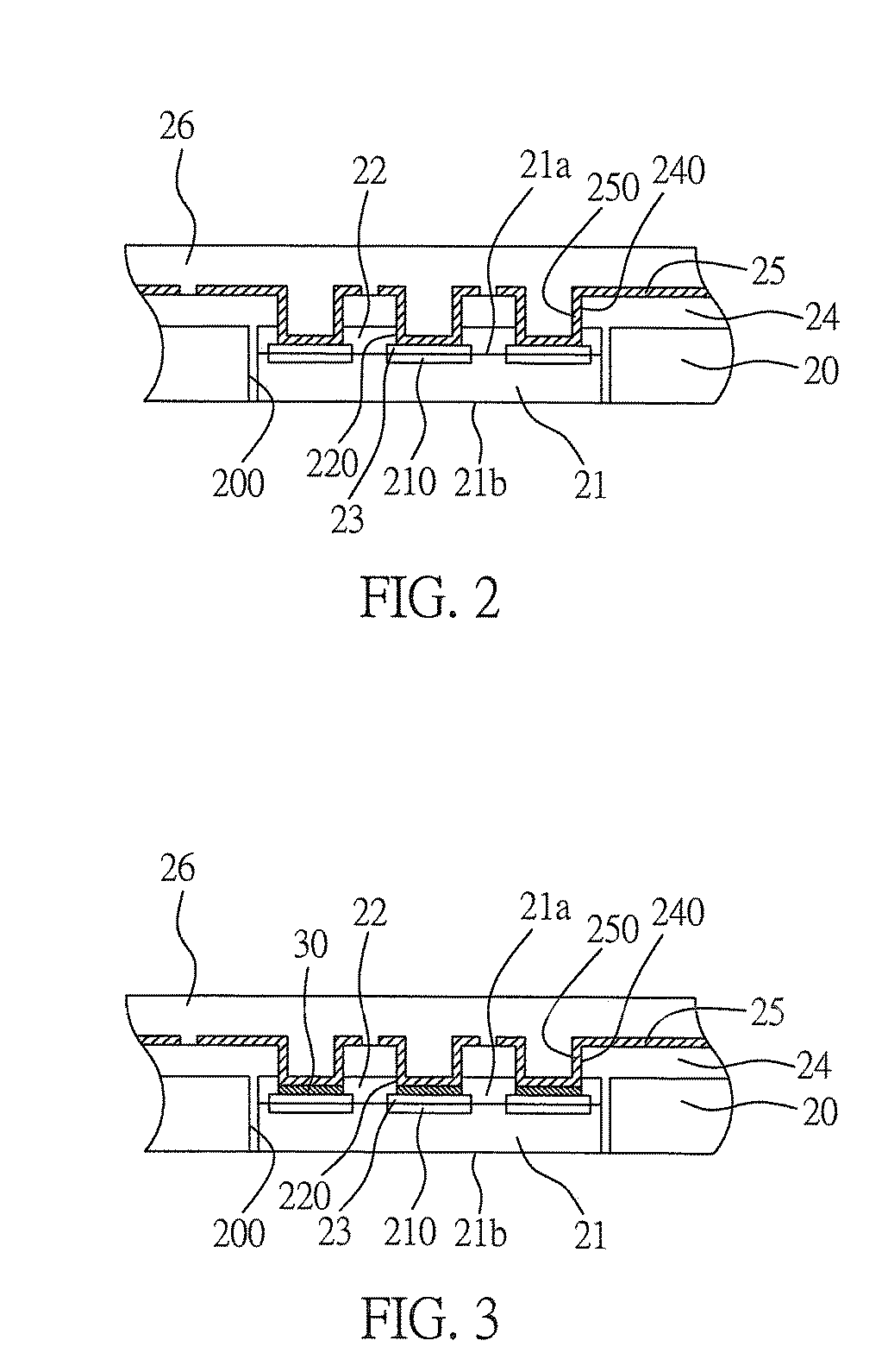
[0031]FIG. 2 is a cross sectional view of a circuit board structure embedded with semiconductor chips of a first embodiment according to the present invention. The circuit board structure comprises a supporting board 20, at least a semiconductor chip 21, a protection layer 22, a metal layer 23, a dielectric layer 24, a circuit layer 25 and a hollow conductive via 250.
[0032]The supporting board 20 is a circuit board or a core board, which the circuit board has completed a former circuit manufacturing process. The core board is made of a metal or non-metal material. At least a cavity 200 is formed in the supporting board 20 for receiving the semiconductor chip 21.
[0033]The semiconductor chip 21 comprises an active surface 21a and a non-active surface 21b opposing to the active surface 21a. A plurality of the electrode pads 210 are formed on the active surface 21a.
[0034]The protection layer 22 is formed on the active surface 21a of the semiconductor chip 21. A plurality of openings 22...
second embodiment
[0040]FIG. 3 is a cross sectional view of a circuit board structure embedded with semiconductor chips of a second embodiment according to the present invention.
[0041]Compared with the circuit board structure of the first embodiment, the circuit board structure of the second embodiment further comprises a buffer metal layer 30.
[0042]The buffer metal layer 30 is formed between the hollow conductive via 250 and the metal layer 23. According to the second embodiment, the buffer metal layer 30 is a copper layer. Therefore, if the metal layer 23 in not thick enough, the thickened buffer metal layer 30 can serve as a stop layer for a laser ablating process for forming the openings (i.e. blind vias) of the dielectric layer 24, and the electrode pads 210 covered under the buffer metal layer 30 can be protected from damages.
third embodiment
[0043]FIG. 4 is a cross sectional view of a circuit board structure embedded with semiconductor chips of a third embodiment according to the present invention.
[0044]Compared with the circuit board structure of the first embodiment, the circuit board structure of the third embodiment further comprises a circuit build-up structure 40 formed on the dielectric layer 24 and the circuit layer 25.
[0045]The circuit build-up structure 40 comprises at least a dielectric layer 400, a circuit layer 402 stacked on the dielectric layer 400, and a fully-plated metal via 404 formed in the dielectric layer 400 for electrically connecting the circuit layer 402 to the circuit layer 25. Of course, another hollow conductive via (not shown) can be used for serving as an electric signal transmission route between the circuit layer 402 and the circuit layer 25.
[0046]The dielectric layer 400 is fully filled in the hollow conductive via 250. Through the design of the hollow conductive via 250, the dielectric...
PUM
 Abstract
Description
Claims
Application Information
 - R&D
- Intellectual Property
- Life Sciences
- Materials
- Tech Scout
- Unparalleled Data Quality
- Higher Quality Content
- 60% Fewer Hallucinations
Browse by: Latest US Patents, China's latest patents, Technical Efficacy Thesaurus, Application Domain, Technology Topic, Popular Technical Reports.
© 2025 PatSnap. All rights reserved.Legal|Privacy policy|Modern Slavery Act Transparency Statement|Sitemap|About US| Contact US: help@patsnap.com