
Eureka
For R&D, Eureka makes reading and utilizing patents & technical documents easy.
Eureka AIR
Designed for self-driven R&D workflows. Generate viable solutions, solve complex R&D challenges, empower your innovation with AI.

Eureka Materials
Designed for material experts only. Revolutionize your material R&D, from search, analyze, to developing new materials.

TechResearch
Generate reliable direction feasibility study reports for your R&D in just a few steps.

TechSeek
Discover and master advanced knowledge NOW. Basics, ideas, possibilities, all at once.

TechMind
As an expert in R&D Theories, TechMind can generates customized viable solutions instantly.

TechRisk
Analyze your overall solution with one click, know your potential R&D risks in advance.

TechMonitor
Get weekly tech updates, stay abreast of the latest tech innovations and key insights.
LED display apparatus
- Summary
- Abstract
- Description
- Claims
- Application Information
AI Technical Summary
Benefits of technology
Problems solved by technology
Method used
Image

Examples
example 1
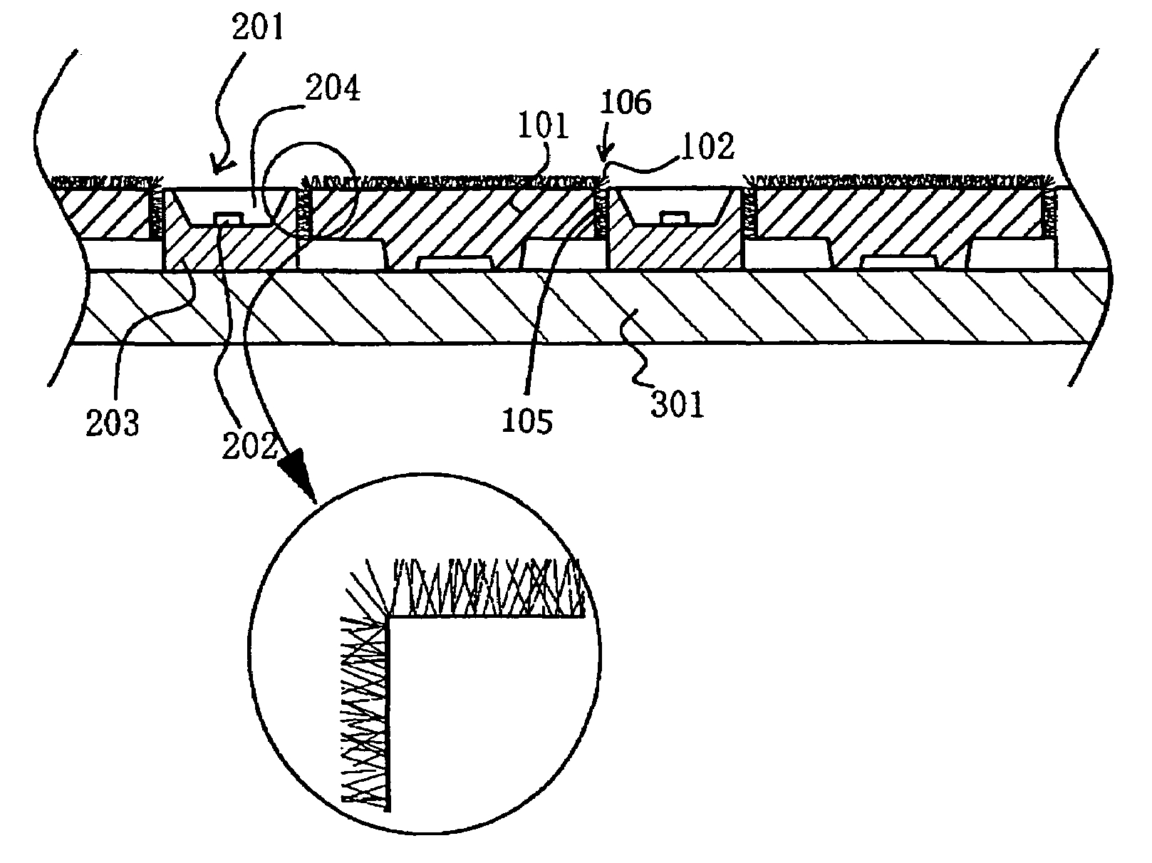
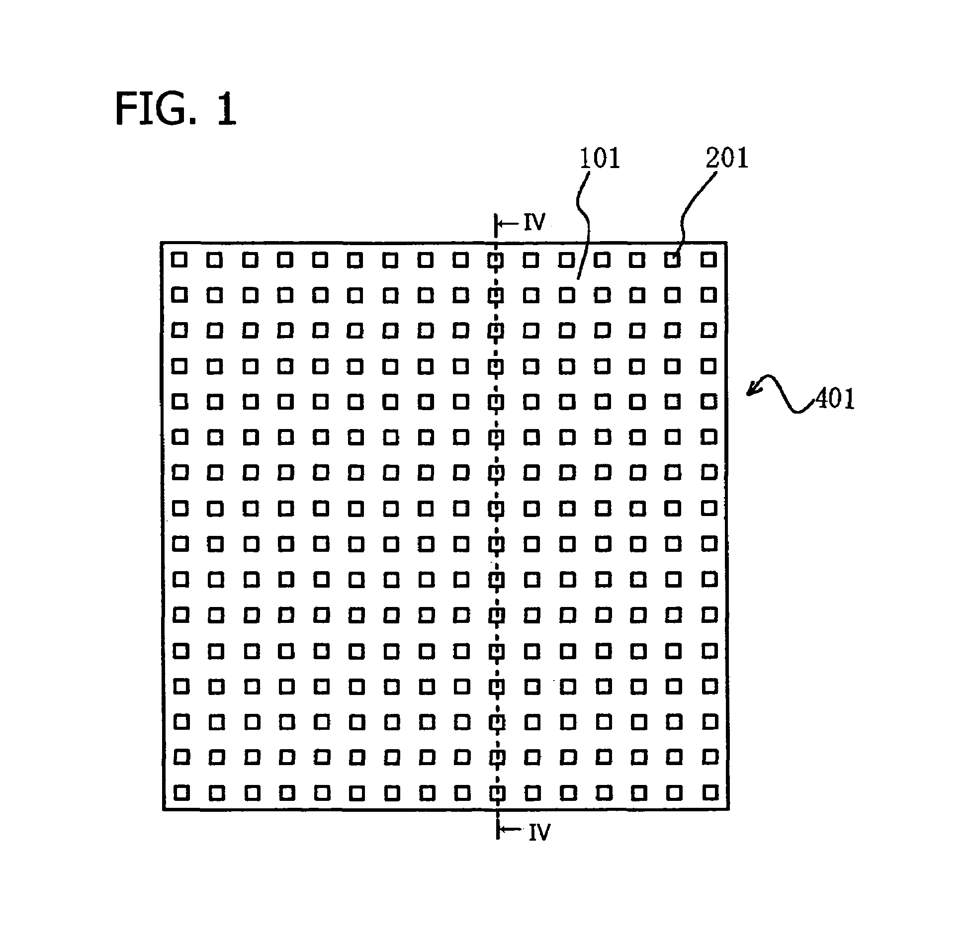
[0091]First, on a circuit board 301 having a size of 160 mm by 160 mm and made of a glass fiber reinforced epoxy resin provided with a conductive pattern, 256 pieces of the light-emitting diodes 201 were arranged in a matrix at regular intervals of 10 mm. The light-emitting diodes 201 were placed on the conductive pattern of the circuit board 301 with solder provided therebetween and were then allowed to pass through a flow soldering apparatus. As a result, the conductive pattern and the light-emitting diodes 201 were fixed and electrically connected to each other.
[0092]As the light-emitting diodes 201 arranged on the circuit board, SMD type light-emitting diodes having a size of 3 mm by 3 mm were used which were formed by the steps of placing light-emitting elements 202 capable of emitting red, green, and blue colors in respective package members 203 made of a polyphthalamide resin, and filling the packages with mold members 204 made of an epoxy resin.
[0093]Next, on the circuit boa...
example 2
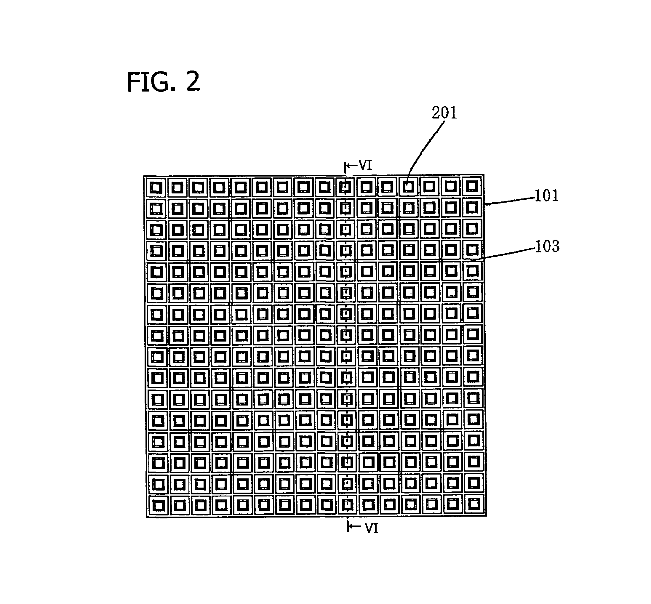
[0099]An LED display apparatus according to Example 2 was obtained by disposing 16 pieces of the LED units 401 shown in FIG. 2 which were formed in the same manner as that described in Example 1. The mask member 101 having a thickness of approximately 1.8 mm was formed in accordance with the circuit board 301 having a size of approximately 160 mm by 160 mm, and the fine projections 102 formed on the mask member 101 had a length of 0.3 mm. In addition, the light-emitting diodes 201 placed on the circuit board 301 each had a size of 3 mm by 3 mm.
[0100]As shown in a schematic, enlarged, cross-sectional view in FIG. 6, the side surfaces 105 of the openings formed in the mask member 101 were inclined side surfaces facing the observation side. The fine projections 102 were formed of flocks of a black polyester material and were provided on the inclined side surfaces 105 of the openings approximately perpendicular thereto. In addition, at the lower portion (circuit board side) of the incli...
example 3
[0102]The LED display unit 401 shown in FIG. 3 was obtained in the same manner as that described in Examples 1 and 2. The mask member 101 having a thickness of approximately 1.8 mm was formed in accordance with the circuit board 301 having a size of approximately 160 mm by 160 mm, and the fine projections 102 formed on the mask member 101 had a length of 0.3 mm. In addition, the light-emitting diode 201 placed on the circuit board 301 had a size of 3 mm by 3 mm.
[0103]On the observation-side surface of the mask member 101 disposed on the circuit board 301, as shown in a schematic, enlarged, cross-sectional view in FIG. 11, louvers 104 were formed having a height of 3 mm and extending in the lateral direction over the entire surface. Since the louvers 104 defined the light-emitting diodes 201 as being formed of individual dots, and also interfered with incident outside light, the image contrast could be improved. As a result, the emission light was brilliant. In addition, since the fi...
PUM
 Abstract
Description
Claims
Application Information
 - R&D Engineer
- R&D Manager
- IP Professional
- Industry Leading Data Capabilities
- Powerful AI technology
- Patent DNA Extraction
Browse by: Latest US Patents, China's latest patents, Technical Efficacy Thesaurus, Application Domain, Technology Topic, Popular Technical Reports.
© 2024 PatSnap. All rights reserved.Legal|Privacy policy|Modern Slavery Act Transparency Statement|Sitemap|About US| Contact US: help@patsnap.com