Method of resin encapsulation, apparatus for resin encapsulation, method of manufacturing semiconductor device, semiconductor device and resin material

a technology of resin encapsulation and resin material, which is applied in the direction of semiconductor devices, semiconductor/solid-state device details, coatings, etc., can solve the problems of high viscosity, difficult for the gas in the melted resin to escape to the outside, and the speed of melted resin introduction, so as to reduce the possibility of generating defective resin mold products and efficiently use resin materials.

Active Publication Date: 2006-06-06
SOCIONEXT INC +1
View PDF14 Cites 19 Cited by
  • Summary
  • Abstract
  • Description
  • Claims
  • Application Information

AI Technical Summary

Benefits of technology

[0012]The present invention was made to solve the above described problems and its object is to reduce possibility of generating defective resin mold products and to efficiently use resin material, when electronic components mounted on a board is resin-encapsulated.

Problems solved by technology

First, it has become more likely that the wire is deformed or disconnected because of the flow of the melted resin introduced into the cavity. Further, it has become more likely that adjacent wires are undesirably brought into contact with each other. In order to solve such problems, it may be helpful to decrease the speed of introduction of the melted resin into the cavity. When the speed of introduction of the melted resin is decreased, however, the melted resin that is being introduced comes to have higher viscosity. This makes it difficult for the gas in the melted resin to escape to the outside. Accordingly, voids or unfilled portions tend to result in the set resin mold.
This increases the possibility of voids or unfilled portions mentioned above.
It is also noted that the resin may undesirably set on the resin flow path.
The resin set on the resin flow path is discarded, and therefore, the conventional method of resin encapsulation involves the problem of waste of resin material.

Method used


Image

  • Method of resin encapsulation, apparatus for resin encapsulation, method of manufacturing semiconductor device, semiconductor device and resin material
  • Method of resin encapsulation, apparatus for resin encapsulation, method of manufacturing semiconductor device, semiconductor device and resin material
  • Method of resin encapsulation, apparatus for resin encapsulation, method of manufacturing semiconductor device, semiconductor device and resin material

Examples


first embodiment

[0041]Referring to FIGS. 1A to 3B, the method of resin encapsulation in accordance with the first embodiment will be described.

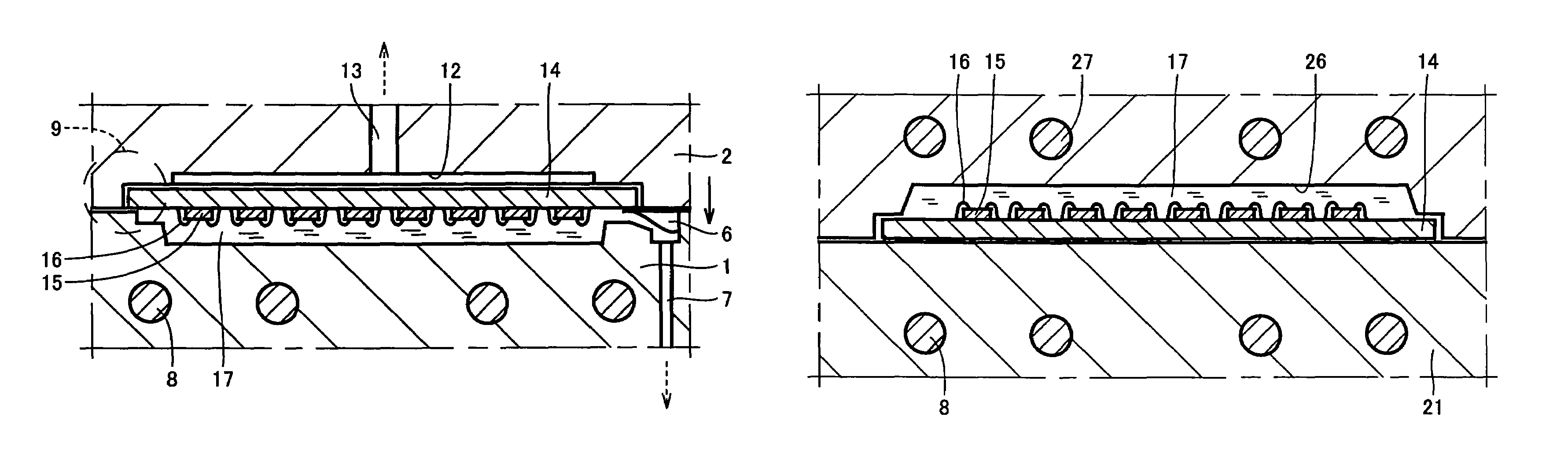
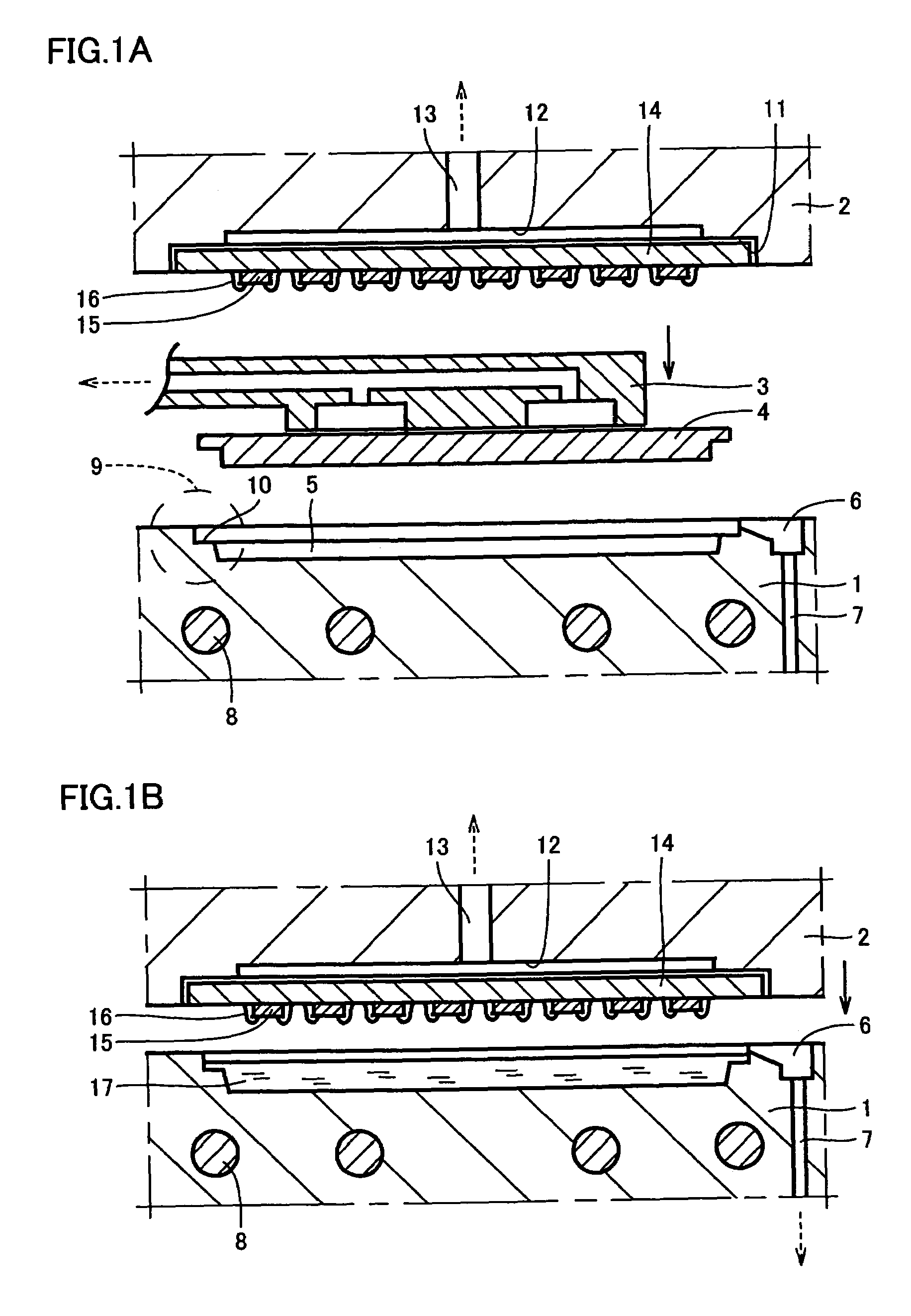
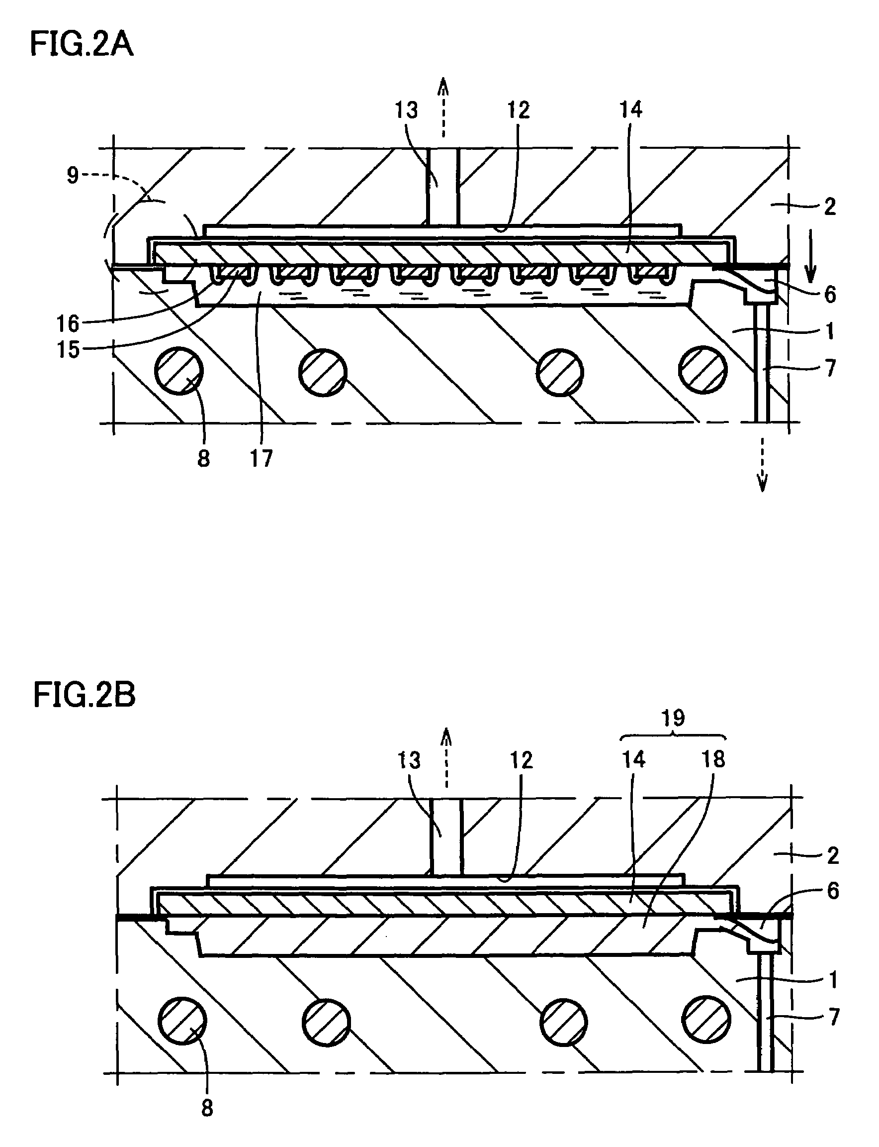
[0042]As can be seen from FIGS. 1A and 1B, in the resin encapsulating apparatus used for the method of resin encapsulation of the present embodiment, a mold pair is provided that has a lower mold 1 and an upper mold 2 opposing to each other. Further, the resin encapsulating apparatus is further provided with press means (not shown) for opening and closing lower mold 1 and upper mold 2.

[0043]Further, FIG. 1A shows a conveyer unit 3 positioned in a space between lower mold 1 and upper mold 2. By the function of a driving mechanism, not shown, conveyer unit 3 can be inserted to the space between lower mold 1 and upper mold 2, and also by the function of the driving mechanism, conveyer unit 3 can be moved from the space between lower mold 1 and upper mold 2 to the outside of the space. A resin material in the form of a plate is fixed to conveyer unit 3 by adsorp...

second embodiment

[0063]Next, the method of resin encapsulation in accordance with the second embodiment will be described with reference to FIGS. 4A to 5B. FIGS. 4A to 5B show the structure of the resin encapsulating apparatus in accordance with the present embodiment. In each of FIGS. 4A to 5B, portions denoted by the same names as the components of the resin encapsulating apparatus in accordance with the first embodiment described with reference to FIGS. 1A to 3B have the same functions as in the first embodiment, and therefore, description thereof will not be repeated.

[0064]Referring to FIGS. 4A to 5B, in the resin encapsulating apparatus in accordance with the present embodiment, board 14 is placed on lower mold 21. On board 14, resin material 22 is placed. Resin material 22 has such size and shape that correspond to the size and shape of a cavity (which will be described later) formed in upper mold 25. Resin material 22 has a flat portion 23 and edge portions 24. As can be seen from FIGS. 4A an...


PUM

PropertyMeasurementUnit
conductiveaaaaaaaaaa
sizeaaaaaaaaaa
timeaaaaaaaaaa

Abstract

First, a board is placed on a board mounting portion with a lower mold and an upper mold being opened. Then, a resin material having such size and shape that correspond to the size and shape of a cavity formed in the lower mold is fitted in the cavity. Thereafter, the resin material is heated resulting in melted resin. Thereafter, the lower mold and the upper mold are closed, with a space formed by the upper mold and the lower mold being reduced in pressure. As a result, chips and wires are immersed in the melted resin. Thereafter, the melted resin is set, so that a resin mold product including the board and the set resin is formed.

Description

BACKGROUND OF THE INVENTION[0001]Field of the Invention[0002]The present invention relates to a method and the like for resin-encapsulation of electronic components on a board.[0003]Description of the Background Art[0004]A conventional method of resin encapsulation, used in manufacturing a semiconductor package as an example of a resin mold product having electronic components mounted on a board will be outlined in the following.[0005]In the conventional method of resin encapsulation, first, a printed circuit (wiring) board (hereinafter simply referred to as a board) having semiconductor chips (hereinafter simply referred to as chips) as exemplary electronic components mounted thereon is prepared. Thereafter, on one of a pair of molds having one mold and the other mold positioned opposed to each other, the board is placed. Then, the mold pair is closed. Thereafter, through a resin flow path, melted resin is introduced into a cavity provided in the other mold of the mold pair. At thi...

Claims


Application Information

Patent Timeline
Patent Type & Authority Patents(United States)
IPC IPC(8): H01L21/44H01L21/56H01L23/02
CPCH01L21/565H01L24/97H01L2924/01068H01L2224/48091H01L2224/48227H01L2224/97H01L2924/01029H01L2924/01033H01L2924/01082H01L2924/01006H01L2924/01005H01L2924/00014H01L2224/85H01L2924/15787H01L2924/181H01L2924/00H01L23/02
Inventor URAGAMI, HIROSHINAKAGAWA, OSAMUFUJINO, KINYATAKASE, SHINJITOKUYAMA, HIDEKIMEGURO, KOICHINISHINO, TORUHAYASAKA, NOBORU
Owner SOCIONEXT INC
Why Eureka
Try Eureka