Method and architecture for reducing the power consumption for memory devices in refresh operations

a memory device and power consumption technology, applied in information storage, static storage, digital storage, etc., can solve the problems of reducing the power consumption further in the standby mode, activating the periphery array circuit of all four quadrants, etc., and achieve the effect of reducing the power consumption of memory devices and reducing the standby power requirements of memory devices

Inactive Publication Date: 2006-06-06
INNOMEMORY LLC
View PDF29 Cites 73 Cited by
  • Summary
  • Abstract
  • Description
  • Claims
  • Application Information

AI Technical Summary

Benefits of technology

[0013]The objects, features and advantages of the present invention include providing a method and / or architecture for reducing the power consumption of memory devices during background operations, such as memory cell refresh operations, that may (i) reduce standby power requirements of a memory device, (ii) refresh one or more sections of a memory array, (iii) activate the support circuits for sections being refreshed, (iv) leave inactive the support circuits for sections not being refreshed and / or (v) perform parity checking and / or housekeeping operations on one or more sections of a memory array.

Problems solved by technology

However, since conventional dynamic semiconductor memory devices are configured to refresh all the memory cells, reducing the power consumption further (e.g., several hundred microamperes) in the standby mode has been difficult.
A disadvantage of the conventional approach is that the periphery array circuits of all four quadrants are activated when less than the full array 26 requires refreshing.

Method used


Image

  • Method and architecture for reducing the power consumption for memory devices in refresh operations
  • Method and architecture for reducing the power consumption for memory devices in refresh operations
  • Method and architecture for reducing the power consumption for memory devices in refresh operations

Examples


Embodiment Construction

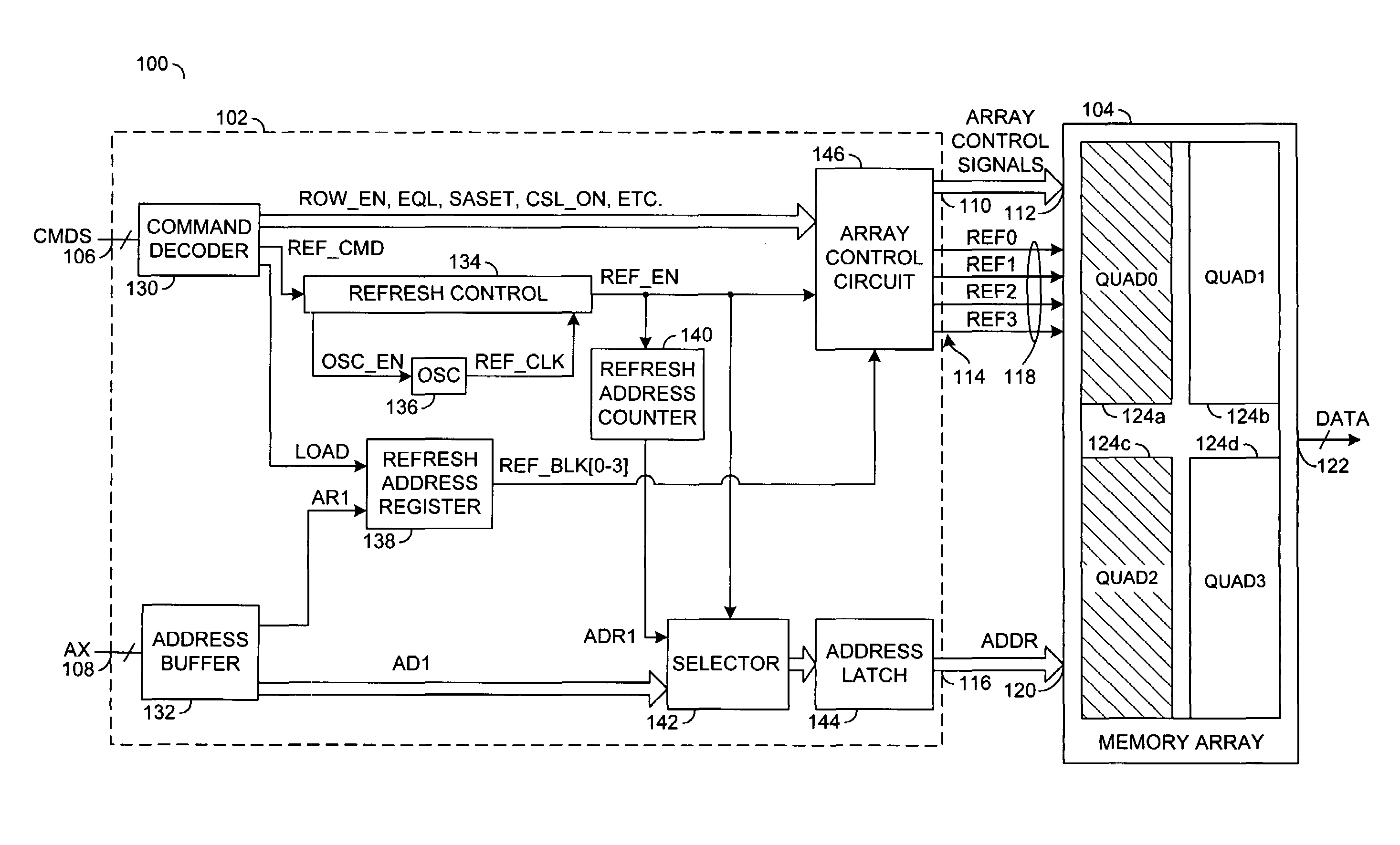
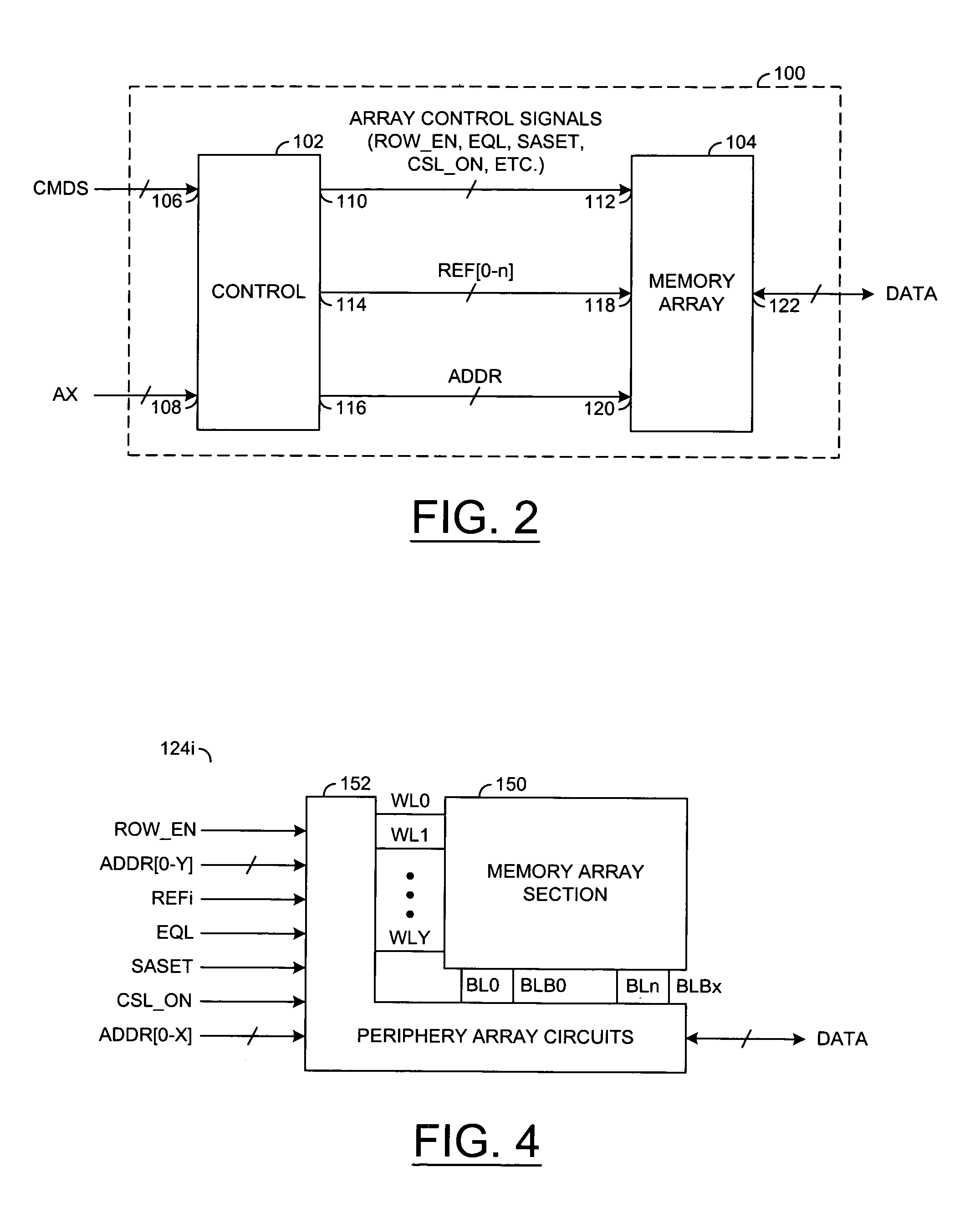
[0022]Referring to FIG. 2, a block diagram of a circuit 100 is shown in accordance with a preferred embodiment of the present invention. The circuit 100 may be implemented, in one example, as a memory device configured to perform refresh operations on all or a subset (portion) of the memory cells of the memory device. The circuit 100 may comprise a circuit (block) 102 and a circuit (block) 104. The circuit 102 may be implemented as a control circuit. The circuit 104 may be implemented as a memory array. The memory array 104 may be implemented with a plurality of sections. Each of the sections may comprise a number of memory cells and periphery array circuitry configured to access the memory cells. The memory cells are generally arranged in rows and columns. During a refresh operation, the circuit 102 may be configured to (i) enable the periphery array circuitry that corresponds to the sections being refreshed and (ii) disable the periphery array circuitry that corresponds to the sec...


PUM


Abstract

A method for reducing power consumption during background operations in a memory array with a plurality of sections comprising the steps of (i) controlling the background operations in one or more sections of the memory array in response to one or more control signals and (ii) presenting the one or more control signals and one or more decoded address signals to one or more periphery array circuits of the one or more sections.

Description

[0001]This is a continuation of U.S. Ser. No. 10 / 090,850, filed Mar. 4, 2002, now U.S. Pat. No. 6,618,314.FIELD OF THE INVENTION[0002]The present invention relates to a method and / or architecture for refreshing a memory device generally and, more particularly, to a method and / or architecture for reducing the power consumption for memory devices in refresh operations.BACKGROUND OF THE INVENTION[0003]Data (i.e., a “1” or a “0”) is stored in a 1T memory cell as a voltage level. A “1” can be stored as a high voltage level which can decrease due to leakage. A “0” can be stored as a voltage level of zero volts which can increase due to leakage. Because of leakage, the 1T memory cell uses a periodic refresh to maintain the detected voltage level stored in the cell.[0004]A refresh operation of a memory chip involves a wordline activation that, together with a sensing operation, restores the data stored in the memory cell. When the chip is in an active mode, the current used for refreshing t...

Claims


Application Information

Patent Timeline
Patent Type & Authority Patents(United States)
IPC IPC(8): G11C7/00G11C11/406
CPCG11C11/406
Inventor FISCUS, TIMOTHY E.CHAPMAN, DAVID E.PARENT, RICHARD M.
Owner INNOMEMORY LLC
Why Eureka
Try Eureka