Ultra-wideband antenna

a band-wideband, ultra-wideband technology, applied in the field of antennas, can solve the problems of destructive interference with the initial current distribution, severe attenuation of the radiation efficiency of the antenna, and the inability of the antenna to respond, so as to achieve the effect of reducing interference and facilitating integration

Active Publication Date: 2006-06-13
IND TECH RES INST
View PDF6 Cites 54 Cited by
  • Summary
  • Abstract
  • Description
  • Claims
  • Application Information

AI Technical Summary

Benefits of technology

[0005]The present invention has been made to overcome the aforementioned drawback of the conventional ultra-wideband antennas. The primary objective of the present invention is ...

Problems solved by technology

Around the center frequency of the antenna's notched frequency band, strong out-of-phase currents surround the outer and inner perimeters of the second slot, causing a destructive interference with...

Method used


Image

  • Ultra-wideband antenna
  • Ultra-wideband antenna
  • Ultra-wideband antenna

Examples


first embodiment

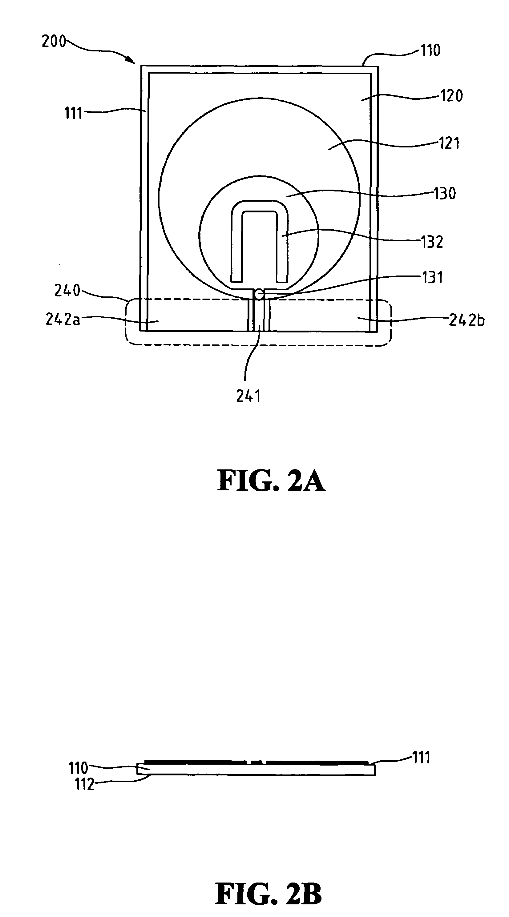
[0026]FIG. 2a is a schematic top view of an ultra-wideband antenna according to the present invention. FIG. 2b is a schematic side view of the ultra-wideband antenna of FIG. 2a.

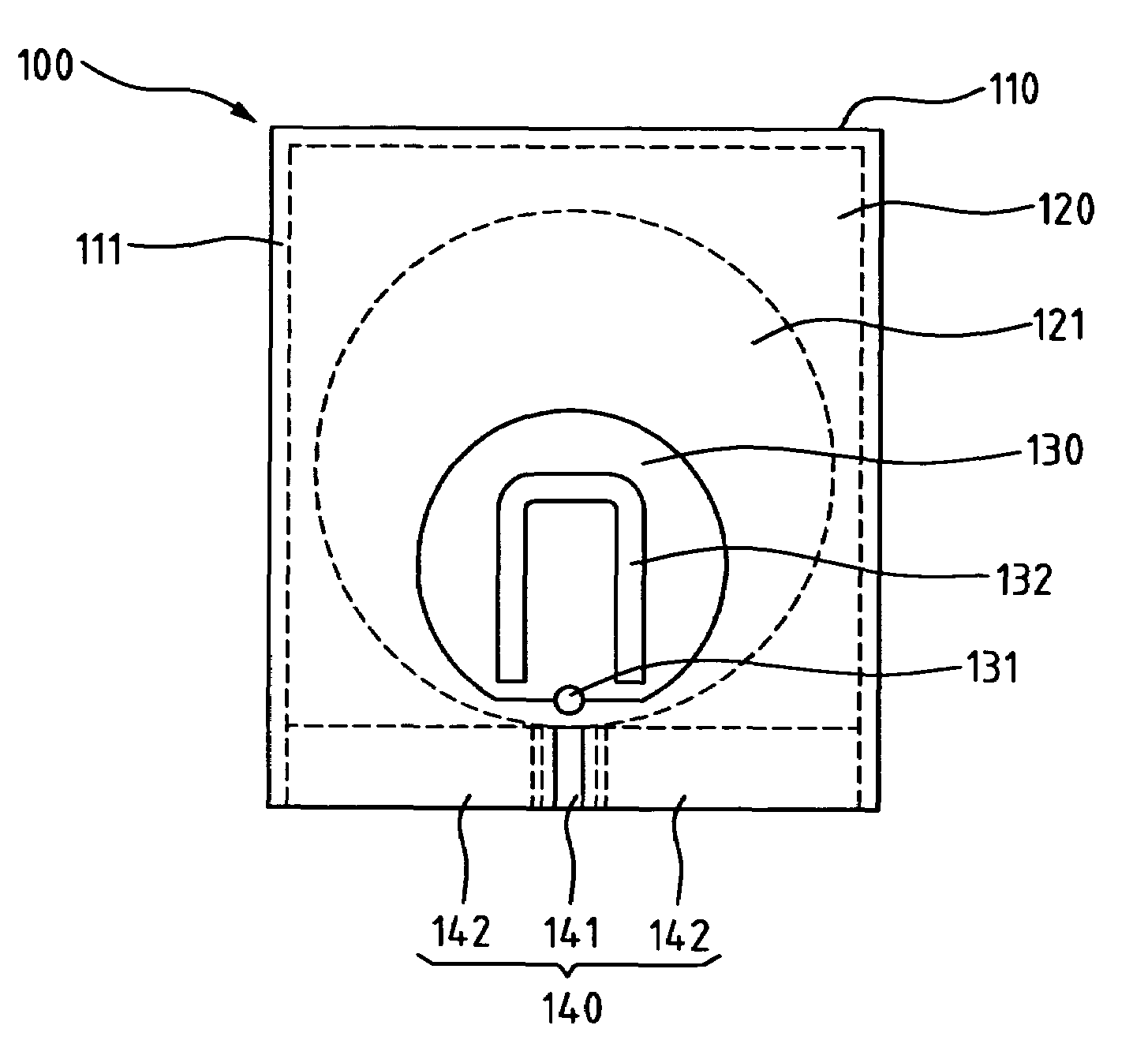
[0027]As illustrated, the first embodiment adopts a co-planar waveguide feed-line 240 whose signal wire is a central metal wire 241 and whose grounding unit includes a first feed-line ground plate 242a and a second feed-line ground plate 242b. The ultra-wideband antenna 200 according to the present embodiment comprises a dielectric substrate 110, a ground plate 120, a metal plate 130, and the co-planar waveguide feed-line 240. The dielectric substrate 110 has a first surface 111 and a second surface 112. Both the ground plate 120 and the metal plate 130 are formed on the first surface 111 of the dielectric substrate 110. The ground plate 120 has a first slot 121. The metal plate 130 is located inside the first slot 121, and has a feed-point 131 and a second slot 132. The co-planar waveguide feed-line 240 is ...

second embodiment

[0032]FIG. 7a is a schematic top view of an ultra-wideband antenna according to the present invention. FIG. 7b is a schematic bottom view of the ultra-wideband antenna of FIG. 7a. FIG. 7c is a schematic side view of the ultra-wideband antenna of FIG. 7a.

[0033]As illustrated, the second embodiment adopts a microstrip feed-line 740 whose signal wire is a metal wire 741 and whose grounding unit is a feed-line ground plate 742. The ultra-wideband antenna 700 according to the present embodiment comprises a dielectric substrate 110, a ground plate 120, a metal plate 130, and the microstrip feed-line 740. The dielectric substrate 110 has a first surface 111 and a second surface 112. The ground plate 120 having a first slot 121 is formed on the second surface 112 of the dielectric substrate 110. The metal plate 130 is formed on the first surface 111 of the dielectric substrate 110 and, within a region corresponding the inside of the fist slot 121, has a feed-point 131 and a U-shaped second...

third embodiment

[0034]FIG. 8a is a schematic top view of an ultra-wideband antenna according to the present invention. FIG. 8b is a schematic side view of the ultra-wideband antenna of FIG. 8a.

[0035]As illustrated, the third embodiment adopts a coaxial feed-line 840 whose signal wire is a central wire 841 and whose grounding unit is an external ground element 742. The ultra-wideband antenna 800 according to the present embodiment comprises a dielectric substrate 110, a ground plate 120, a metal plate 130, and the coaxial feed-line 840. The present embodiment shares a similar structure with that of the first embodiment except that, besides the difference of the feed-line, the ground plate 120 of the present embodiment further has a ground-point 822. The central wire 841 is connected to the feed-point 131. The external ground element 842 is connected to ground-point 822 of the ground plate 120. In the present embodiment, the second slot 132, fed by the coaxial feed-line 840, is a curved one (i.e., a...


PUM


Abstract

An ultra-wideband (UWB) antenna is provided. It comprises a dielectric substrate, a ground plate, a metal plate, and a transmission line. The ground plate formed on the dielectric substrate has a first slot thereon. The metal plate formed on the dielectric substrate has a feed-point and a second slot thereon. The total length of the second slot is about a half-wavelength at the desired notched frequency for the UWB antenna. By embedding the second slot of a suitable length on the metal plate resided in the first slot, a band notched characteristic is achieved for the antenna in the 5 GHz band, thereby overcoming the problem of signal interference with the UWB operations. The disclosed antenna and the circuitry for the antenna system are easily integrated. With the simple structure, the fabrication cost for the antenna is also reduced.

Description

FIELD OF THE INVENTION[0001]The present invention generally relates to antennas, and more particularly to a band-notched ultra-wideband (UWB) antenna.BACKGROUND OF THE INVENTION[0002]In recent years, transmission speed and information capacity of wireless communications are increased in an exponential rate, driven by the increasing demand for short-range wireless communications, wireless local area networks (WLANs), and personal mobile communications devices. For these related applications, Federal Communications Commissions (FCC) specified in February 2002 that ultra-wideband communications technologies are to be used for commercial communications and for high-speed, low-power and short-range communications. In addition, Institute of Electrical and Electronic Engineering (IEEE) also proposed a new standard, IEEE 802.15 WPAN (wireless personal area network), for mobile communications consumer devices to provide high-speed and low-power ultra-wideband communications. However, over th...

Claims


Application Information

Patent Timeline
IPC IPC(8): H01Q13/10H01Q1/38H01Q1/48H01Q5/00H01Q5/28H01Q9/40
CPCH01Q1/38H01Q5/28H01Q13/10H01Q9/40
Inventor TANG, CHIA-LUNWONG, KIN-LUSU, SAOU-WENLIN, YUAN-CHIH
Owner IND TECH RES INST
Why Eureka
Try Eureka