Method and apparatus using interferometric metrology for high aspect ratio inspection

a high aspect ratio, interferometric metrology technology, applied in the direction of measurement devices, scientific instruments, instruments, etc., can solve the problems of difficult to distinguish from other defects with similar contrast, difficult to detect dark defects sitting in dark structures, and difficulty in wafer inspection challenges for chipmakers, etc., to achieve better alignment

Active Publication Date: 2006-06-13
KLA TENCOR TECH CORP
View PDF9 Cites 89 Cited by
  • Summary
  • Abstract
  • Description
  • Claims
  • Application Information

AI Technical Summary

Benefits of technology

[0012]In another embodiment, an adjustable magnification module is located in the optical path between the interferometric microscope module and the image sensor for adjusting the size of the interference image onto the image sensor. By using such a system,

Problems solved by technology

With intensity based systems it is difficult to detect dark defects sitting in dark structures or to differentiate from other defects with similar contrast.
HARI provides difficult wafer inspection challenges to chipmakers, especially as the integrated circuits become smaller.
Because the background is darker, slight perturbations may not easily be discriminated against the background.
Furthermore, dark structures provide relatively low signal levels.
Moreover, other background noise, such as from misalignment between images for example

Method used


Image

  • Method and apparatus using interferometric metrology for high aspect ratio inspection
  • Method and apparatus using interferometric metrology for high aspect ratio inspection
  • Method and apparatus using interferometric metrology for high aspect ratio inspection

Examples


Embodiment Construction

[0029]Reference will now be made in detail to specific embodiments of the invention. Examples of these embodiments are illustrated in the accompanying drawings. While the invention will be described in conjunction with these specific embodiments, it will be understood that it is not intended to limit the invention to these embodiments. On the contrary, it is intended to cover alternatives, modifications, and equivalents as may be included within the spirit and scope of the invention as defined by the appended claims. In the following description, numerous specific details are set forth in order to provide a thorough understanding of the present invention. The present invention may be practiced without some or all of these specific details. In other instances, well known process operations have not been described in detail in order not to unnecessarily obscure the present invention.

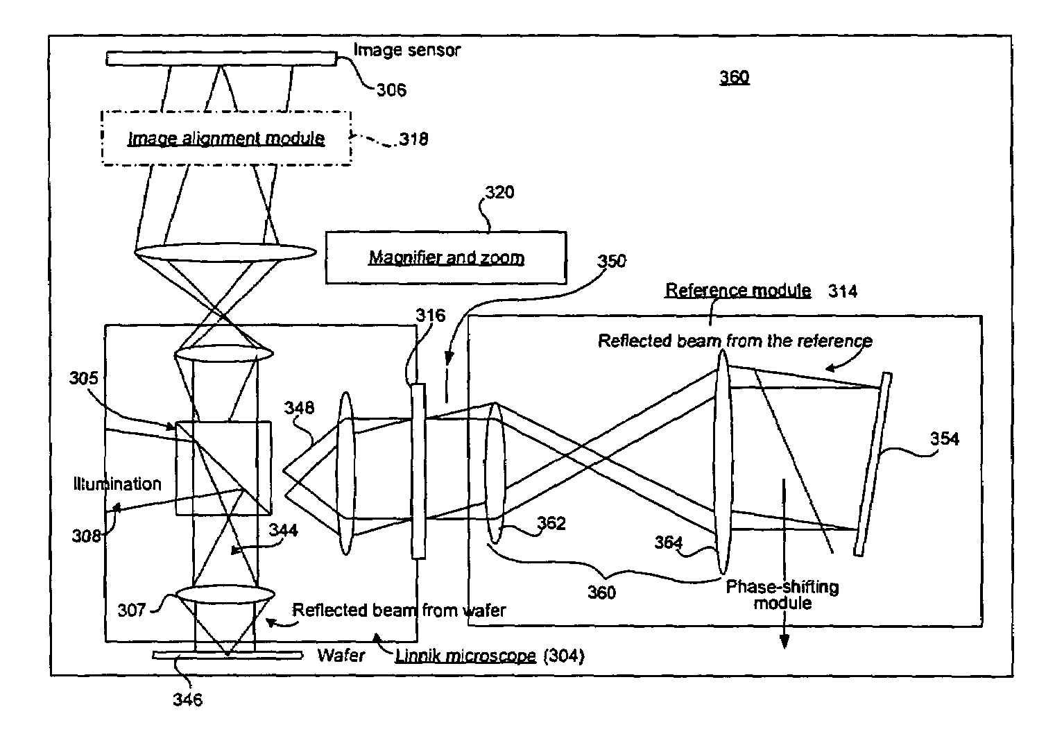
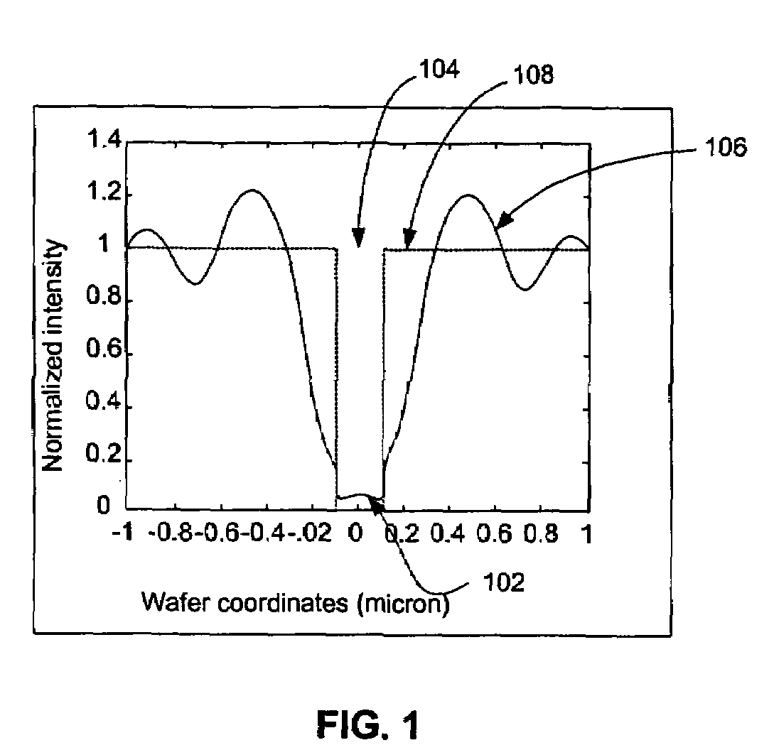
[0030]The present invention applies interferometric techniques to defect inspection on semiconductor wa...


PUM


Abstract

In one embodiment, the present invention provides an interferometric inspection system for inspecting semiconductor samples. The system includes at least one illumination source for generating an illumination beam and an interferometric microscope module for splitting the illumination beam into a test beam directed to the semiconductor sample and a reference beam directed to a tilted reference mirror. The beams are combined to generate an interference image at an image sensor. The tilted reference mirror is tilted at a non-normal angle with respect to the reference beam that is incident on the mirror to thereby generate fringes in the interference image. The system also includes an image sensor for acquiring the interference image from the interferometric microscope module and generates an inherence signal. The system further includes a processing module configured to generate complex field information corresponding to the sample from the interference image signal and an alignment module located in the optical path between the interferometric module and the image sensor. In another embodiment, the processing module is configured to generate complex field information from either spatial fringe analysis or temporal fringe analysis performed on the interference image signal.

Description

CROSS-REFERENCE TO RELATED APPLICATIONS[0001]This application claims priority of U.S. Provisional Patent Application No. 60 / 414,725, filed 27 Sep. 2002, which application is incorporated herein by reference in its entirety for all purposes. This application is filed concurrently with and related to the following patent application: United States Nonprovisional application Ser. No. 10 / 673,058, entitled “METHOD AND APPARATUS USING MICROSCOPIC AND INTERFEROMETRIC BASED DETECTION” naming Hwang et al. as inventors. The above-referenced US patent application is incorporated herein by reference in its entirety for all purposes.BACKGROUND OF THE INVENTION[0002]The present invention relates generally to methods and systems for inspecting defects on wafers, masks, and reticles. More particularly, the present invention relates to optical inspection systems and techniques.[0003]In a conventional optical inspection system, defects are detected by subtracting a reference image from a test image t...

Claims


Application Information

Patent Timeline
IPC IPC(8): G01B9/02
CPCG01B11/2441G01N21/95607G01N21/9501G03H2001/0456
Inventor HWANG, SHIOW-HWEIFU, TAO-YI
Owner KLA TENCOR TECH CORP
Why Eureka
Try Eureka