Creation of high mobility channels in thin-body SOI devices

a technology of soi devices and high mobility, applied in semiconductor/solid-state device manufacturing, basic electric elements, electric devices, etc., can solve the problem of difficult growth of strained silicon film onto silicon-on-insulator wafers

Inactive Publication Date: 2006-06-27
INTEL CORP
View PDF8 Cites 15 Cited by
  • Summary
  • Abstract
  • Description
  • Claims
  • Application Information

AI Technical Summary

Problems solved by technology

Growing strained silicon film onto silicon-on-insulator wafer, however, is difficult since

Method used


Image

  • Creation of high mobility channels in thin-body SOI devices
  • Creation of high mobility channels in thin-body SOI devices
  • Creation of high mobility channels in thin-body SOI devices

Examples


Embodiment Construction

[0014]In the following, for purposes of explanation, numerous details are set forth in order to provide a thorough understanding of the present invention. However, it will be apparent to one skilled in the art that theses specific details are not required in order to practice the present invention.

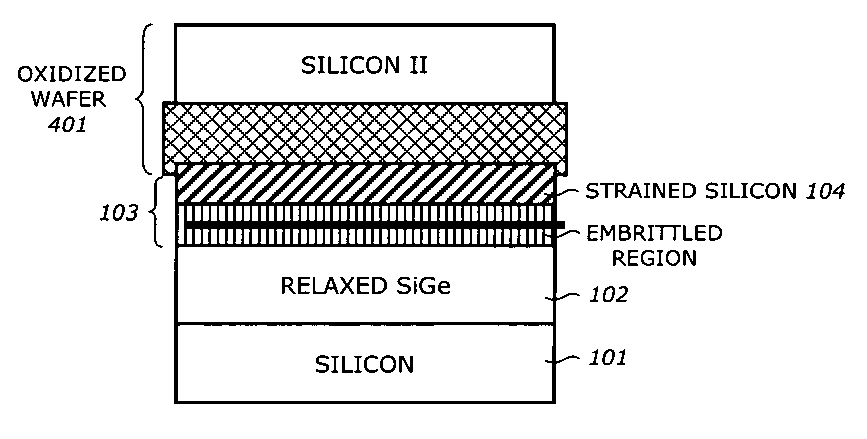
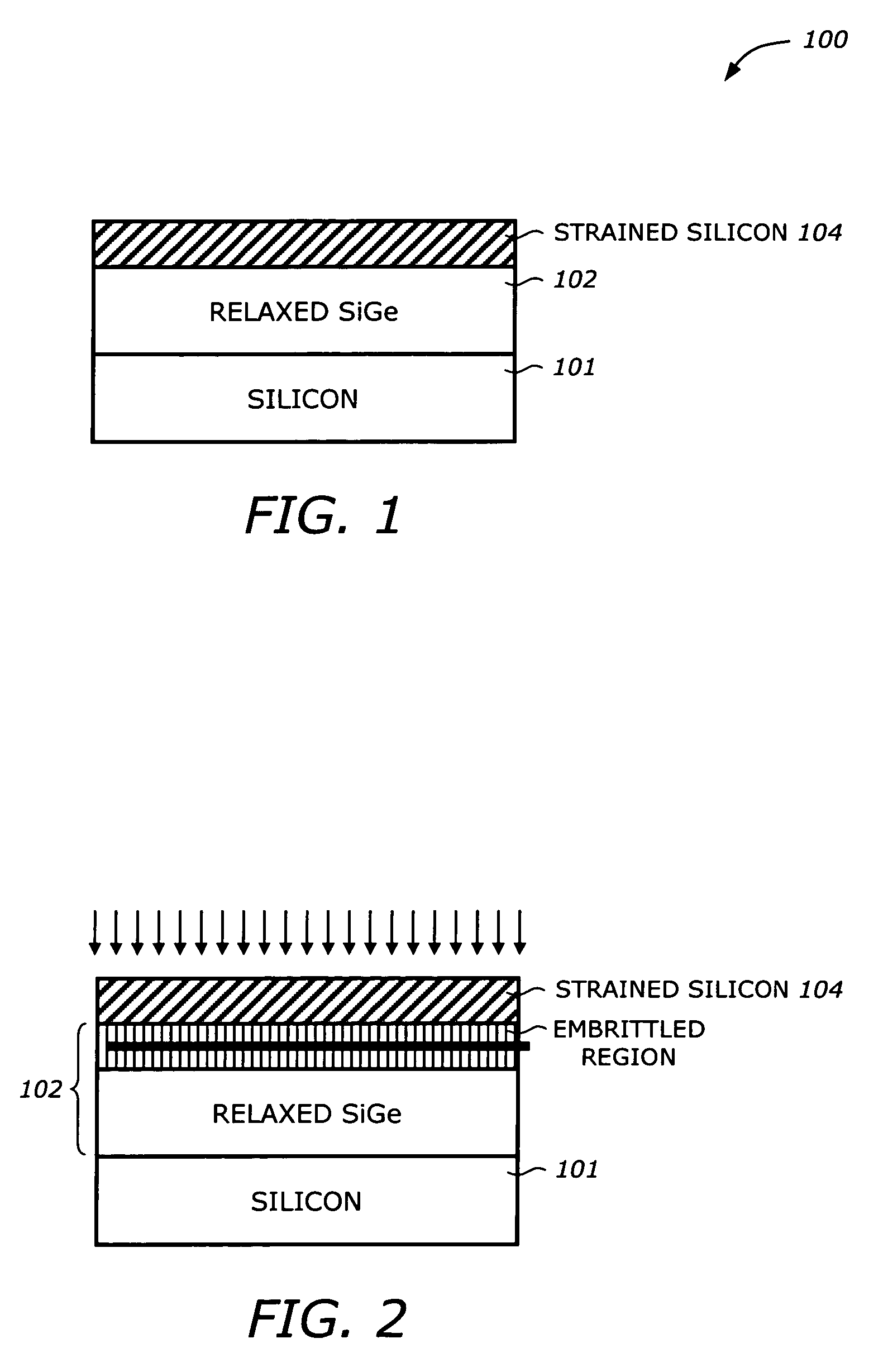
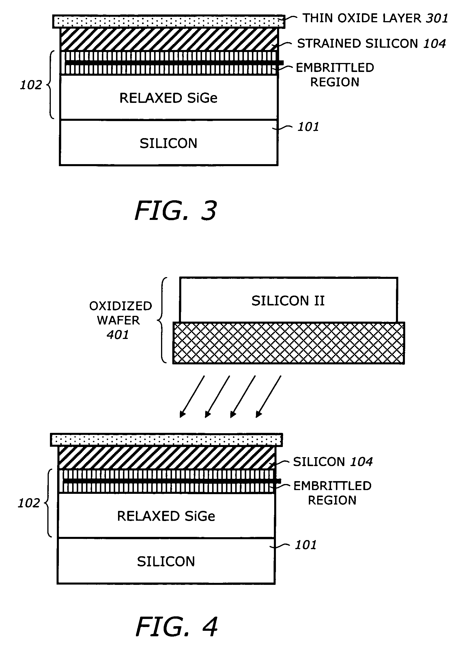
[0015]FIG. 1 is a diagram illustrating a sectional view of a wafer having a stack structure of a conventional substrate with a strained silicon layer. The wafer 100 may includes heteroepitaxial layers of a starting silicon platform (e.g., substrate) 101, a silicon germanium (SiGe) alloy graded relaxed buffer layer 102, and a strained silicon layer 104.

[0016]The relaxed SiGe layer 102 is formed upon or deposited on top the silicon substrate 101. The strained silicon layer 104 is then formed on the relaxed SiGe layer 102. In one embodiment, the relaxed SiGe layer 102, and the strained silicon layer 104 are formed by an epitaxial growth process. In other words, the process includes epitaxial ...


PUM


Abstract

A method for fabricating a strained silicon film to a silicon on insulation (SOI) wafer. A layer of oxide is deposited onto a wafer that has a stack structure of a first base substrate, a layer of relaxed film-and a second layer of strained film. The SOI wafer has a stack structure of a second base substrate and a layer of oxidized film. The SOI wafer is attached to the wafer and is heated at a first temperature. This causes a silicon dioxide (SiO2) dangling bond to form on the second base substrate of the SOI wafer, transferring the strained film from one wafer to the other.

Description

CROSS-REFERENCES TO RELATED APPLICATIONS[0001]This is a Divisional Application of U.S. patent application No. 09 / 895,579, filed Jun. 29, 2001, now U.S. Pat. No. 6,717,213. This Divisional Application claims the benefit of the U.S. patent application No. 09 / 895,579.FIELD OF THE INVENTION[0002]This invention relates to a method for fabricating strain on a wafer. In particular, the invention relates to a method for fabricating strain on a silicon-on-insulator (SOI) wafer.DESCRIPTION OF THE RELATED ART[0003]The mobility of the carriers in a device is directly related to the its current. The higher the current the faster the device is operated. Devices can be built as bulk devices, devices on silicon on insulator (SOI) or any other types. Each type has its own characteristics that make it attractive. As these devices are scaled down, one of the characteristics that may be of interest is the speed of metal oxide semiconductor (MOS) transistors. One way to make a speedier transistor is to ...

Claims


Application Information

Patent Timeline
IPC IPC(8): H01L21/00H01L21/762
CPCH01L21/76254H01L21/02381H01L21/0245H01L21/02532H01L21/02664H01L21/0251
Inventor DOYLE, BRIAN S.ROBERDS, BRIAN E.
Owner INTEL CORP
Why Eureka
Try Eureka