Suppression of leakage current in image acquisition
a leakage current and image acquisition technology, applied in the direction of coupling device connection, radiation control device, instruments, etc., can solve the problems of leakage current flowing into the tfts, deteriorating image acquisition accuracy, and lowering light sensitivity
- Summary
- Abstract
- Description
- Claims
- Application Information
AI Technical Summary
Benefits of technology
Problems solved by technology
Method used
Image
Examples
first embodiment
1. First Embodiment
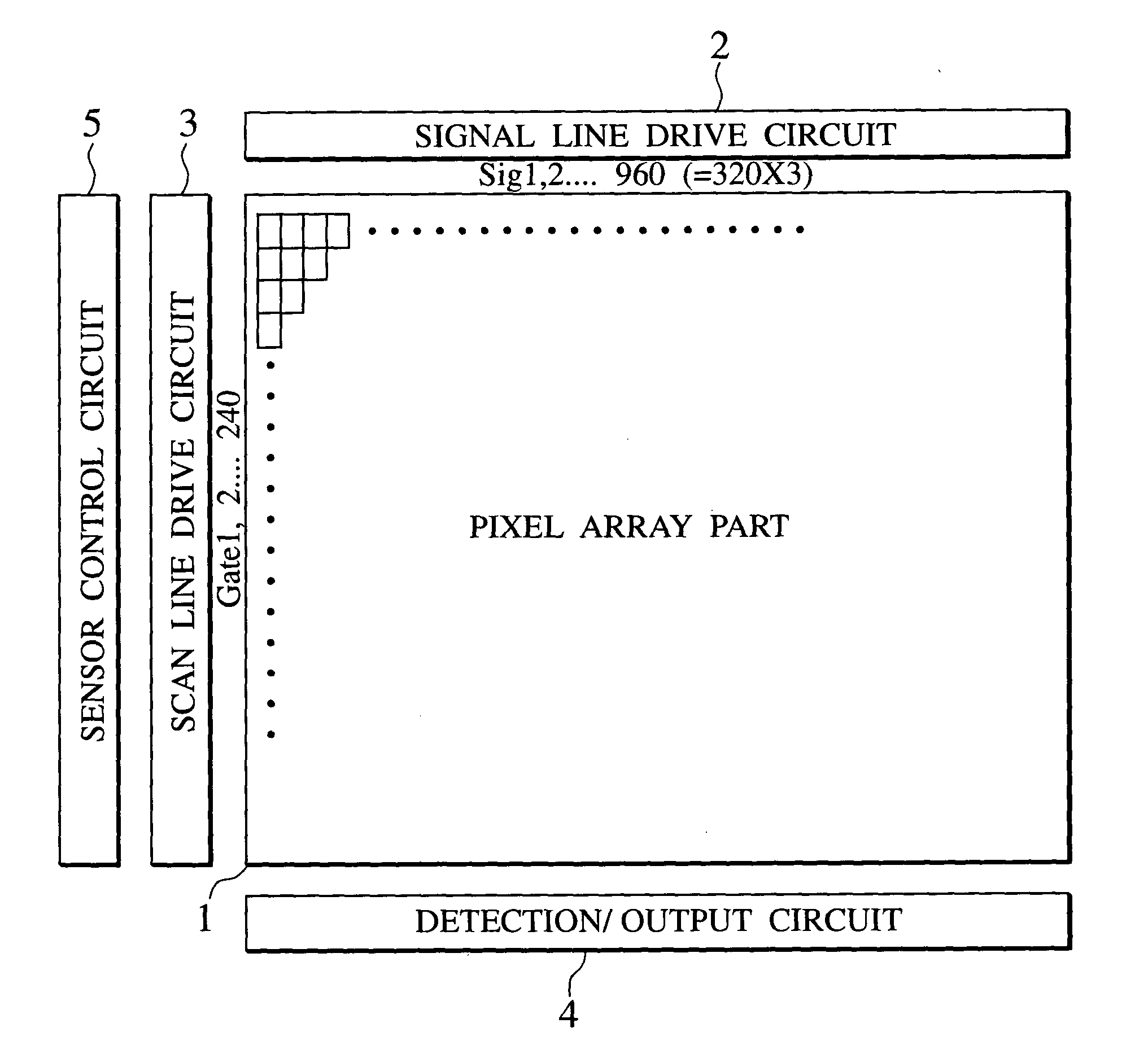
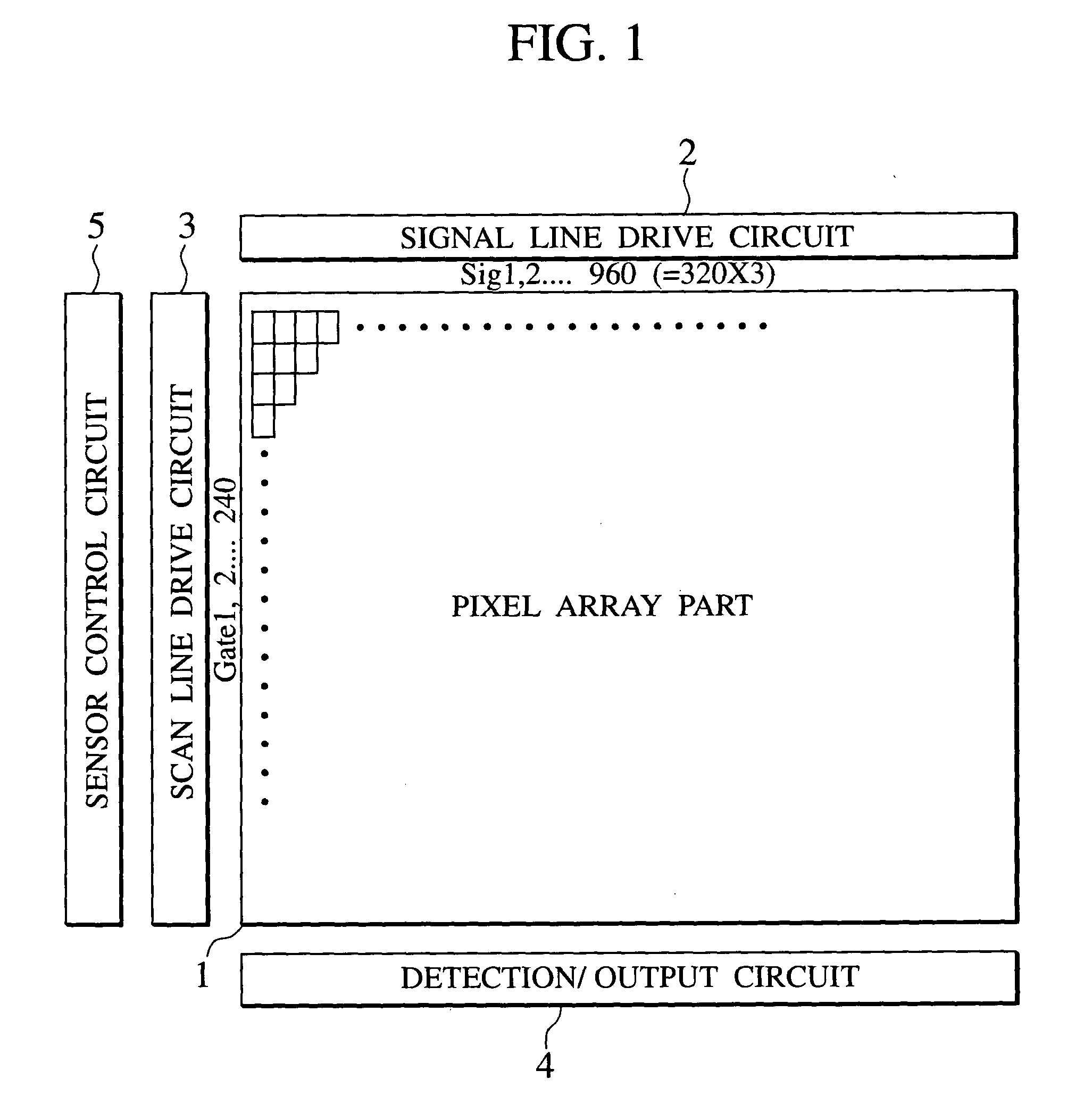
[0053] As shown in a circuit block diagram of FIG. 1, a display device of a first embodiment includes, on an insulating substrate made of glass: a pixel array part 1 in which pixels are disposed at the respective intersections of signal lines and scan lines; a signal line drive circuit 2 which drives the signal lines; a scan line drive circuit 3 which drives the scan lines; a detection / output circuit 4 which acquires and outputs an image; and a sensor control circuit 5 which controls sensors for image acquisition. This detection / output circuit 4 includes analog / digital conversion circuits for image acquisition and parallel / serial conversion circuits for output. These above-described circuits constitute an array substrate.
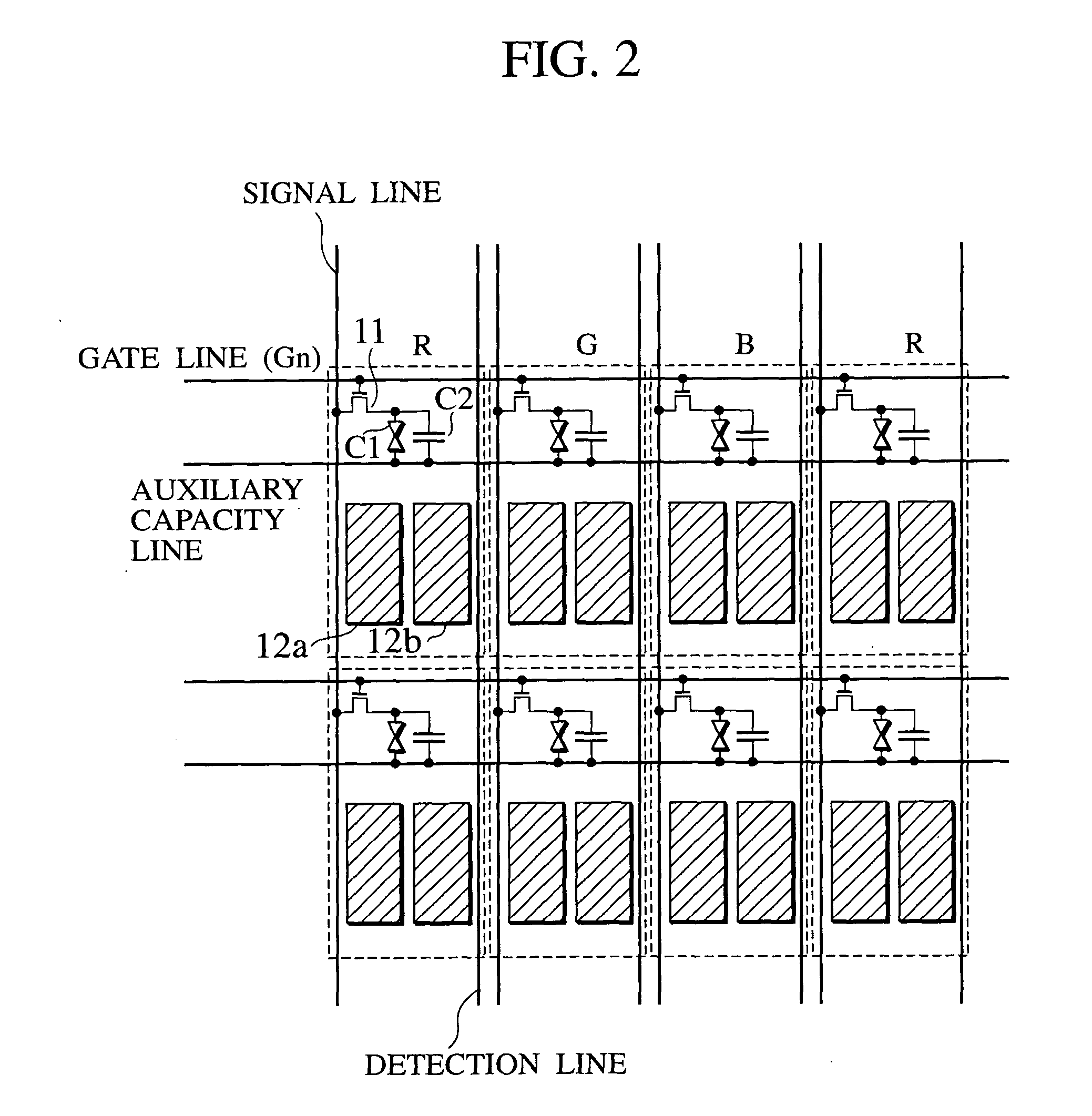
[0054] As shown in a detailed circuit block diagram of FIG. 2, the pixel array part 1 has: switching elements 11 for driving pixels, which are formed at the respective intersections of the signal lines and the scan lines (gate lines) that are inst...
second embodiment
2. Second Embodiment
[0096] As shown in a cross-sectional view of FIG. 14, in an optical sensor diode according to a second embodiment, a silicon film 102 is formed to have a thickness of about 150 nm on a glass insulating substrate 101 by plasma CVD. The silicon film 102 is formed of silicon nitride, silicon oxide or lamination thereof. On the silicon film 102, a semiconductor layer 110 made of polysilicon is formed so as to have a thickness of about 50 nm. This semiconductor layer 110 is formed by disposing a p region 111 with p-type impurities injected therein, an i region 112 including hardly any impurities and a n region 113 with n-type impurities injected therein adjacently to each other in this order. In the p region 111, boron is injected, for example, at a high concentration of about 1.times.10.sup.19 atm / cm.sup.3. In the n region 113, phosphorous is injected at a high concentration of about 1.times.10.sup.19 atm / cm.sup.3. The i region 112 may be a region to which boron or p...
third embodiment
3. Third Embodiment
[0106] As shown in the circuit diagram of FIG. 19, in a circuit configuration of a third embodiment, a bias voltage Vnp is supplied to the cathode electrode 116 of the optical sensor diode 100 and a gate voltage Vgp is supplied to the gate electrode 114. The anode electrode 115 is connected to ground.
[0107] The graph of FIG. 20 shows current-voltage characteristics of the optical sensor diode 100 when a fixed voltage is applied as the gate voltage Vgp in the circuit diagram shown in FIG. 19. This graph shows a characteristic 405 in the case of irradiating no light onto the optical sensor diode 100 and a characteristic 406 in the case of irradiating light. This graph shows a good characteristic in which a current ratio of a current at the time of irradiating light (hereinafter referred to as an "irradiation current") to a current at the time of no irradiation (hereinafter referred to as a "non-irradiation current"), which is irradiation current / non-irradiation curr...
PUM
 Abstract
Description
Claims
Application Information


