Semiconductor structure and fabrication method thereof

a technology of semiconductors and semiconductors, applied in the direction of semiconductor devices, electrical devices, transistors, etc., can solve the problems of weak control ability the stress layer may be easily damaged, and the weakening of the gate of the transistor to the channel of the transistor

Active Publication Date: 2019-02-28
SEMICON MFG INT (SHANGHAI) CORP +1
View PDF10 Cites 4 Cited by
  • Summary
  • Abstract
  • Description
  • Claims
  • Application Information

AI Technical Summary

Problems solved by technology

Thus, the control ability of the gate of the transistor to the channel of the transistor has become weaker and weaker.
However, when the GAA structure is introduced into the transistor having the stress layer, the stress layer may be easily damaged.

Method used


Image

  • Semiconductor structure and fabrication method thereof
  • Semiconductor structure and fabrication method thereof
  • Semiconductor structure and fabrication method thereof

Examples


Embodiment Construction

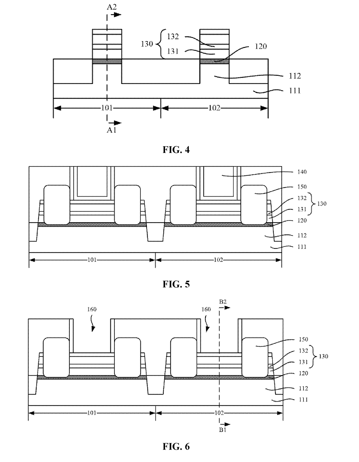
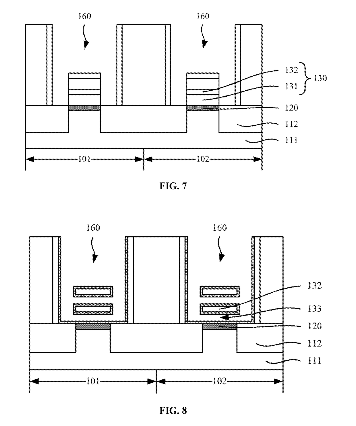
[0013]Reference will now be made in detail to exemplary embodiments of the disclosure, which are illustrated in the accompanying drawings. Wherever possible, the same reference numbers will be used throughout the drawings to refer to the same or like parts.

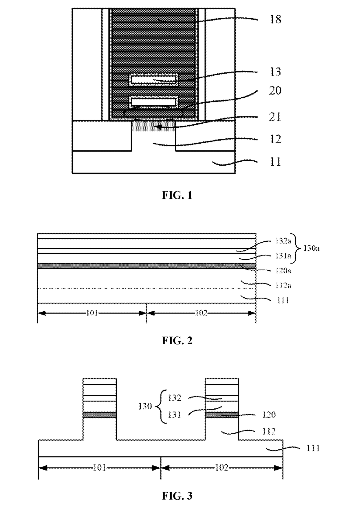
[0014]FIG. 1 illustrates a gate-all-around (GAA) semiconductor structure. As shown in FIG. 1, the GAA semiconductor structure includes a semiconductor substrate 11, a fin 12 protruding from a surface of the semiconductor substrate 11, a channel layer 13 formed on the fin 12 and isolated from the fin 12, and an all-around gate 18 formed on the fin 12 and surrounding the channel layer 13.

[0015]Because the all-around gate 18 surrounds the channel layer 13, the all-around gate 18 fills the gap (i.e., the structure circled as 20 in FIG. 1) between the channel layer 13 and the fin 12. When the all-around gate 18 receives a signal to turn on the channel of the semiconductor structure, a channel is formed in the channel layer 13, and a pa...


PUM

PropertyMeasurementUnit
semiconductoraaaaaaaaaa
semiconductor structureaaaaaaaaaa
thicknessaaaaaaaaaa

Abstract

Semiconductor structures and fabrication methods are provided. An exemplary fabrication method includes providing a semiconductor substrate having a fin material layer on the semiconductor substrate; forming an isolation material layer having a bandgap greater than a bandgap of the fin material layer on the fin material layer; and forming a stacked channel material layer on the isolation material layer. The stacked channel material layer includes a sacrificial material layer and a channel material layer on the sacrificial material layer. The method also includes etching the stacked channel material layer, the isolation material layer and the fin material layer to form fins protruding from the semiconductor substrate, an isolation layer on the fins and a stacked channel layer on the isolation layer. The stacked channel layer includes a sacrificial layer and a channel layer on the sacrificial material layer.

Description

CROSS-REFERENCES TO RELATED APPLICATIONS[0001]This application claims the priority of Chinese patent application No. 201710727131.3, filed on Aug. 22, 2017, the entirety of which is incorporated herein by reference.FIELD OF THE DISCLOSURE[0002]The present disclosure generally relates to the field of semiconductor manufacturing technologies and, more particularly, relates to semiconductor structures and fabrication methods.BACKGROUND[0003]With the repaid development of semiconductor manufacturing technologies, semiconductor devices have been developed towards higher device density and higher integration level. As basic semiconductor devices, transistors have been widely used. With the continuous increase of the device density and integration level, the channel length of the transistor has been continuously reduced. With the continuous reduction of the channel length of the transistor, the distance between the source and the drain of the transistor has been continuously reduced. Thus,...

Claims


Application Information

Patent Timeline
Patent Type & Authority Applications(United States)
IPC IPC(8): H01L29/423H01L29/786H01L29/66H01L21/306H01L21/3065H01L21/308H01L21/311
CPCH01L29/42392H01L29/78696H01L29/66742H01L29/66545H01L21/30604H01L21/3065H01L21/308H01L21/31116H01L21/31144H01L27/0922H01L29/0607H01L29/7848H01L29/165H01L29/78603H01L21/84H01L21/823878H01L21/8221H01L27/0688
Inventor ZHOU, FEI
Owner SEMICON MFG INT (SHANGHAI) CORP
Why Eureka
Try Eureka